

Temporal logic circuits implementation using a dual cross-inhibition mechanism based on DNA strand displacement
- PMID: 37701285
- PMCID: PMC10493850
- DOI: 10.1039/d3ra03995a
Temporal logic circuits implementation using a dual cross-inhibition mechanism based on DNA strand displacement
Abstract
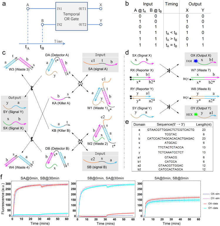
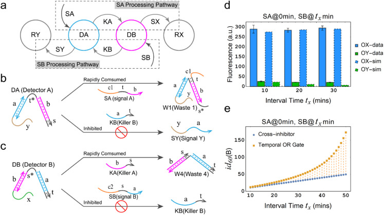
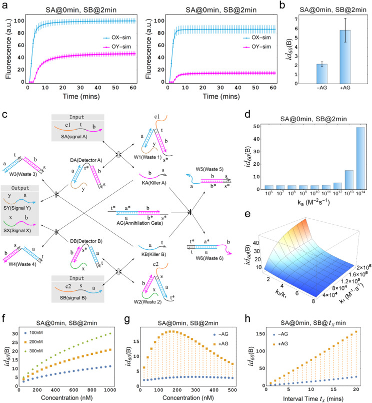
Molecular circuits crafted from DNA molecules harness the inherent programmability and biocompatibility of DNA to intelligently steer molecular machines in the execution of microscopic tasks. In comparison to combinational circuits, DNA-based temporal circuits boast supplementary capabilities, allowing them to proficiently handle the omnipresent temporal information within biochemical systems and life sciences. However, the lack of temporal mechanisms and components proficient in comprehending and processing temporal information presents challenges in advancing DNA circuits that excel in complex tasks requiring temporal control and time perception. In this study, we engineered temporal logic circuits through the design and implementation of a dual cross-inhibition mechanism, which enables the acceptance and processing of temporal information, serving as a fundamental building block for constructing temporal circuits. By incorporating the dual cross-inhibition mechanism, the temporal logic gates are endowed with cascading capabilities, significantly enhancing the inhibitory effect compared to a cross-inhibitor. Furthermore, we have introduced the annihilation mechanism into the circuit to further augment the inhibition effect. As a result, the circuit demonstrates sensitive time response characteristics, leading to a fundamental improvement in circuit performance. This architecture provides a means to efficiently process temporal signals in DNA strand displacement circuits. We anticipate that our findings will contribute to the design of complex temporal logic circuits and the advancement of molecular programming.
This journal is © The Royal Society of Chemistry.
Conflict of interest statement
There are no conflicts to declare.
Figures
Similar articles
-
DNA Strand-Displacement Temporal Logic Circuits.J Am Chem Soc. 2022 Jul 13;144(27):12443-12449. doi: 10.1021/jacs.2c04325. Epub 2022 Jul 2. J Am Chem Soc. 2022. PMID: 35785961 Free PMC article.
-
Erasable and Field Programmable DNA Circuits Based on Configurable Logic Blocks.Adv Sci (Weinh). 2024 Jul;11(26):e2400011. doi: 10.1002/advs.202400011. Epub 2024 May 2. Adv Sci (Weinh). 2024. PMID: 38698560 Free PMC article.
-
Constructing DNA logic circuits based on the toehold preemption mechanism.RSC Adv. 2021 Dec 22;12(1):338-345. doi: 10.1039/d1ra08687a. eCollection 2021 Dec 20. RSC Adv. 2021. PMID: 35424506 Free PMC article.
-
DNA Logic Circuits for Cancer Theranostics.Small. 2022 May;18(20):e2108008. doi: 10.1002/smll.202108008. Epub 2022 Mar 7. Small. 2022. PMID: 35254723 Review.
-
Information processing based on DNA toehold-mediated strand displacement (TMSD) reaction.Nanoscale. 2021 Feb 4;13(4):2100-2112. doi: 10.1039/d0nr07865d. Nanoscale. 2021. PMID: 33475669 Review.
References
-
- Lacroix A. Sleiman H. F. ACS Nano. 2021;15:3631–3645. - PubMed
-
- Platnich C. M. Rizzuto F. J. Cosa G. Sleiman H. F. Chem. Soc. Rev. 2020;49:4220–4233. - PubMed
-
- Wang S. S. Ellington A. D. Chem. Rev. 2019;119:6370–6383. - PubMed
-
- van Roekel H. W. Rosier B. J. Meijer L. H. Hilbers P. A. Markvoort A. J. Huck W. T. de Greef T. F. Chem. Soc. Rev. 2015;44:7465–7483. - PubMed
-
- Qian L. Winfree E. Bruck J. Nature. 2011;475:368–372. - PubMed
LinkOut - more resources
Full Text Sources
Research Materials