

High-throughput dry transfer and excitonic properties of twisted bilayers based on CVD-grown transition metal dichalcogenides
- PMID: 37705802
- PMCID: PMC10496764
- DOI: 10.1039/d3na00371j
High-throughput dry transfer and excitonic properties of twisted bilayers based on CVD-grown transition metal dichalcogenides
Abstract
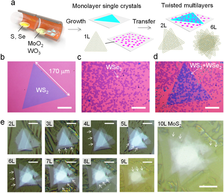
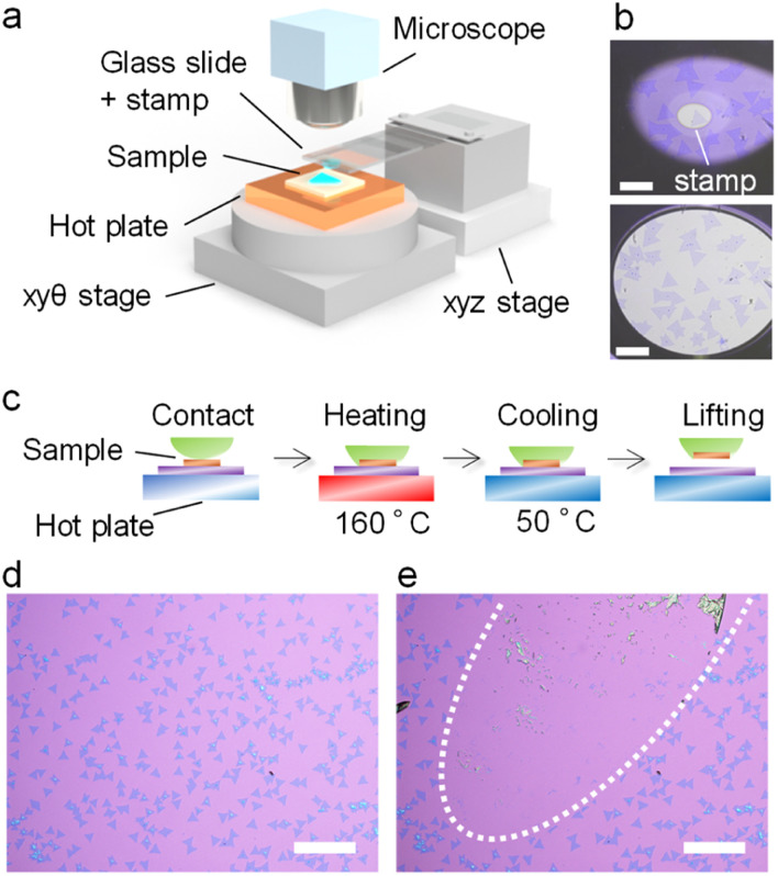
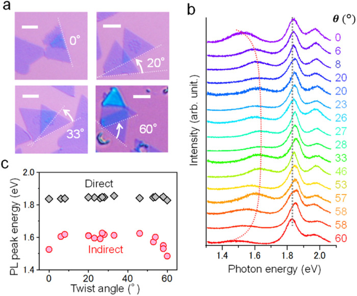
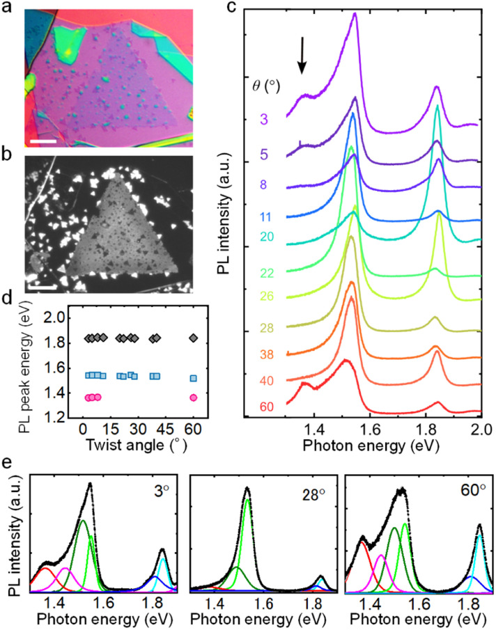
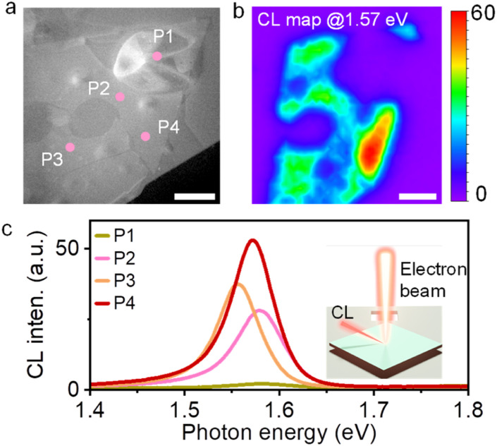
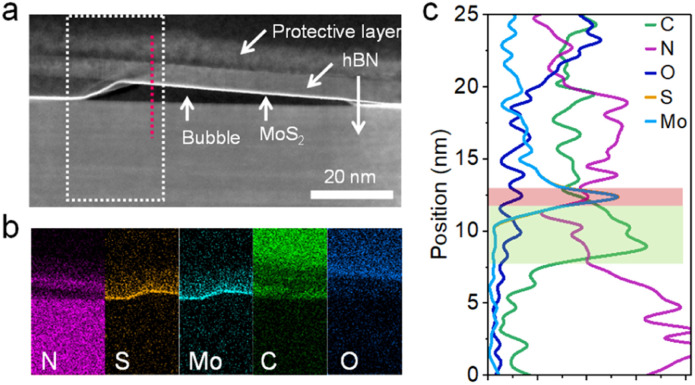
van der Waals (vdW) layered materials have attracted much attention because their physical properties can be controlled by varying the twist angle and layer composition. However, such twisted vdW assemblies are often prepared using mechanically exfoliated monolayer flakes with unintended shapes through a time-consuming search for such materials. Here, we report the rapid and dry fabrication of twisted multilayers using chemical vapor deposition (CVD) grown transition metal chalcogenide (TMDC) monolayers. By improving the adhesion of an acrylic resin stamp to the monolayers, the single crystals of various TMDC monolayers with desired grain size and density on a SiO2/Si substrate can be efficiently picked up. The present dry transfer process demonstrates the one-step fabrication of more than 100 twisted bilayers and the sequential stacking of a twisted 10-layer MoS2 single crystal. Furthermore, we also fabricated hBN-encapsulated TMDC monolayers and various twisted bilayers including MoSe2/MoS2, MoSe2/WSe2, and MoSe2/WS2. The interlayer interaction and quality of dry-transferred, CVD-grown TMDCs were characterized by using photoluminescence (PL), cathodoluminescence (CL) spectroscopy, and cross-sectional electron microscopy. The prominent PL peaks of interlayer excitons can be observed for MoSe2/MoS2 and MoSe2/WSe2 with small twist angles at room temperature. We also found that the optical spectra were locally modulated due to nanosized bubbles, which are formed by the presence of interface carbon impurities. The present findings indicate the widely applicable potential of the present method and enable an efficient search of the emergent optical and electrical properties of TMDC-based vdW heterostructures.
This journal is © The Royal Society of Chemistry.
Conflict of interest statement
There are no conflicts to declare.
Figures
References
LinkOut - more resources
Full Text Sources