Review
. 2024 Feb;36(8):e2304523.
doi: 10.1002/adma.202304523. Epub 2023 Dec 6.

Halide Perovskites and Their Derivatives for Efficient, High-Resolution Direct Radiation Detection: Design Strategies and Applications

Affiliations
Review

Halide Perovskites and Their Derivatives for Efficient, High-Resolution Direct Radiation Detection: Design Strategies and Applications

Kavya Reddy Dudipala et al. Adv Mater. 2024 Feb.

Abstract

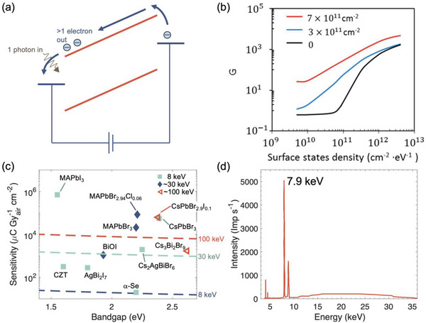
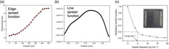
The past decade has witnessed a rapid rise in the performance of optoelectronic devices based on lead-halide perovskites (LHPs). The large mobility-lifetime products and defect tolerance of these materials, essential for optoelectronics, also make them well-suited for radiation detectors, especially given the heavy elements present, which is essential for strong X-ray and γ-ray attenuation. Over the past decade, LHP thick films, wafers, and single crystals have given rise to direct radiation detectors that have outperformed incumbent technologies in terms of sensitivity (reported values up to 3.5 × 10⁶ µC Gyair -1 cm-2 ), limit of detection (directly measured values down to 1.5 nGyair s-1 ), along with competitive energy and imaging resolution at room temperature. At the same time, lead-free perovskite-inspired materials (e.g., methylammonium bismuth iodide), which have underperformed in solar cells, have recently matched and, in some areas (e.g., in polarization stability), surpassed the performance of LHP detectors. These advances open up opportunities to achieve devices for safer medical imaging, as well as more effective non-invasive analysis for security, nuclear safety, or product inspection applications. Herein, the principles behind the rapid rises in performance of LHP and perovskite-inspired material detectors, and how their properties and performance link with critical applications in non-invasive diagnostics are discussed. The key strategies to engineer the performance of these materials, and the important challenges to overcome to commercialize these new technologies are also discussed.

Keywords: charge-carrier kinetics; halide perovskites; imaging; ion migration; perovskite-inspired materials; radiation detectors; stability.


Conflict of interest statement

The authors declare no conflict of interest.

Figures

Figure 1
Figure 1
Application of ionizing radiation for non‐invasive, non‐destructive diagnostics. a) Illustration of the attenuation of common materials to electromagnetic radiation, with the regions categorized as soft and hard X‐rays, and γ‐rays. Reproduced under the terms of the CC‐BY‐3.0 license.[ 31 ] Copyright 2021, The Authors. Published by the Royal Society of Chemistry. b) Sketch of a direct radiation detector (vertical photoconductor structure) operated under reverse bias.[ 43 ] c) Example of an image of a hand taken using X‐rays and an amorphous selenium detector. Reproduced under the terms of the CC‐BY license.[ 44 ] Copyright 2011, The Authors. Published by MDPI. d) Example of a γ‐ray spectrum taken with a CsPbBr3 single crystal detector, showing the resolution of the 662 keV 137Cs peak. Reproduced under the terms of the CC‐BY license.[ 45 ] Copyright 2018, The Authors. Published by Springer Nature.
Figure 2
Figure 2
Rise in performance of lead‐halide perovskite (LHP) and Bi‐based perovskite‐inspired material (PIM) radiation detectors. Plot of a) sensitivity and b) lowest detectable dose rate (LoDD) reported for X‐ray detectors based on single crystal LHPs and Bi‐based PIMs. The sensitivity of commercial‐standard α‐Se is shown (Tables 1 and 3), as is the LoDD of α‐Se (the current medical standard, 5500 nGyair s−1)[ 48 , 49 ] and the best LoDD of scintillators (13 nGyair s−1).[ 51 ] c) Energy resolution of LHP single crystal detectors for 122 keV 57Co, 59.6 keV 241Am and 667 keV 137Cs γ‐rays,[ 52 ] compared to the energy resolution of high purity Ge at 77 K (0.2%) and CZT at room temperature (0.5%).[ 30 ] d) Spatial resolution (at 20% modulation transfer function) of LHPs and Bi‐based PIM X‐ray imagers, compared with the minimum requirements for radiography (5.7 lp mm−1) and mammography (10 lp mm−1).[ 53 ] Please refer to Table 4 for a more detailed discussion of the evolution of spatial resolution in LHP imagers. Data obtained from Ref. [54] Higher sensitivity and spatial resolution are better, while lower LoDD and energy resolution are better. Please note that the reports shown were not all obtained under the same conditions (including dose rate, mean radiation energy, spectrum of radiation source, applied bias). Since each of these parameters influences the performance of radiation detectors, we cannot obtain a direct comparison between each report. But this figure serves as a useful visual guide of what values have been reported. Readers are encouraged to go to Table 3, and the references therein to check the measurement conditions used.
Figure 3
Figure 3
Simplified diagram of a typical direct‐conversion Flat Panel X‐ray Imager based on α‐Se as the X‐ray attenuation layer. Diagram based on Ref. [57] Here, we discuss the attenuating materials used for digital radiography, and the key properties required. A discussion of the interfaces, and how they influence performance and polarization stability is given in Sections 4.6 and 5.3.
Figure 4
Figure 4
Effect of device architecture on photocurrent, and the performance metrics of radiation detectors. a) Comparison of the band diagram of photoconductors (left – symmetric Ohmic electrodes) and photodiodes (right – Schottky contact on the left, and Ohmic contact on the right) placed in reverse bias. In both cases, X‐rays are illuminated through the electrode on the left. For the photoconductor, charge‐carriers can be injected from the electrodes into the semiconductor, such that dark current can match or exceed the photocurrent. For the photodiode, the electrodes impede or block charge‐injection from the electrodes, such that the photocurrent substantially exceeds the dark current. b) Plot of photocurrent against applied bias for perovskite radiation detectors made into the photoconductor and photodiode structure. Reproduced under the terms of the CC‐BY license.[ 75 ] Copyright 2021, The Authors. Published by Elsevier. c) Comparison of the dark currents for perovskite single crystal devices made with symmetric (Au/Au) or asymmetric (Pb/Au) electrodes, d) the sensitivities of Au/MAPbI3/Au vs. Pb/MAPbI3/Au devices under forward and reverse bias, and e) the lowest detectable dose rate (D˙limit) that would be extracted from the Pb/MAPbI3/Au device under reverse (photoconductive gain < 1) or forward bias (photoconductive gain > 1). Panels (c)–(e) reproduced under the terms of the CC‐BY license.[ 43 ] Copyright 2021, The Authors. Published by Springer Nature.
Figure 5
Figure 5
Effects of photoconductive gain, and the sensitivity of X‐ray detectors. a) Illustration of the conventional explanation for photoconductive gain. Only electrons shown for convenience. b) Plot of photoconductive gain (G) against surface state density for a simulated p‐type silicon slab (400 nm thick) for different concentrations of fixed charges. Part (b) reproduced with permission.[ 85 ] Copyright 2018, American Chemical Society. c) Theoretical maximum sensitivity (S 0) calculated from Equation 7 at different X‐ray energies (8 keV, 30 keV, 100 keV) as a function of the bandgap of the attenuation material, shown as dashed lines. The reported sensitivities of lead‐halide perovskite and Bi‐based PIM X‐ray detectors are shown as points, organized based on the approximate peak energy of the X‐ray source. Data shown in Table 3. d) X‐ray spectrum used to measure BiOI detectors, showing that whilst the peak energy is at 7.9 keV, the spectrum had photons at up to 35 keV energy. Part (d) reproduced with permission under the terms of the CC‐BY license.[ 56 ] Copyright 2023, The Authors. AIP Publishing.
Figure 6
Figure 6
Determining the spatial resolution of an X‐ray imager. The a) edge spread function (ESF) is first determined by measuring the photocurrent from the imager across a precisely‐defined edge attenuating the X‐ray source. The first derivative of the ESF is calculated to give b) the line spread function, and a Fourier transform is taken to obtain c) the modulation transfer function vs. the spatial frequency. Reproduced under the terms of the CC‐BY license.[ 69 ] Copyright 2019, The Authors. Published by Springer Nature.
Figure 7
Figure 7
a) Linear attenuation coefficient of established (α‐Se, CdTe) and a selection of emerging radiation detector materials for ionizing radiation. The energy regions used for mammography, digital radiography and computed tomography (CT) scans are highlighted (see Table 1), along with the energies associated with common γ‐ray sources. The attenuation coefficients were calculated using Ref. [113], along with the densities of the materials.[ 54 ] Attenuation efficiency of materials to b) 30 keV and c) 100 keV radiation calculated using the linear attenuation coefficients of these materials.
Figure 8
Figure 8
Defect tolerance and self‐healing of lead‐halide perovskites. a) Plot of the shift in valence band to Fermi level offset from the pristine MAPbI3 thin film sample (ΔE) as a function of the I/Pb ratio. Reproduced with permission.[ 172 ] Copyright 2016, American Chemical Society. b) Photoluminescence quantum yield of CsPbX3 nanocrystals (X = I, Br or Cl), as a function of their concentration. As the concentration is decreased, the surface halide vacancy content increases. Reproduced with permission.[ 173 ] Copyright 2018, American Chemical Society. c) Photographs of triple cation perovskite photovoltaic devices (top) and indium tin oxide (ITO)‐coated glass substrates (bottom) before and after exposure to 2.3 Mrad γ‐rays after 1535 h. d) Proposed mechanism for self‐healing in the perovskite films during γ‐ray exposure. e) Comparison of the normalized power conversion efficiency (PCE) of triple‐cation perovskite photovoltaics versus c‐Si photovoltaics as a function of the radiation dose. Parts (c–e) reproduced with permission.[ 175 ] Copyright 2018, Wiley‐VCH GmbH.
Figure 9
Figure 9
X‐ray detector performance of δ‐CsPbI3 microwires. a) Operational stability of MAPbI3 and δ‐CsPbI3 photoconductors under continuous exposure to X‐rays (45 Gyair s−1 dose rate, 100 kVp). b) Current from δ‐CsPbI3 microwire detectors with and without exposure to 50 kVp X‐rays of different dose rates (labeled in µGyair s−1). c) SNR of the photocurrent under 33.3 nGyair s−1 dose rate at different applied biases. Device structure inset. d) Modulation transfer function to measure the spatial resolution of the δ‐CsPbI3 detectors. Reproduced with permission.[ 53 ] Copyright 2022, Wiley‐VCH GmbH.
Figure 10
Figure 10
Defects and passivation in lead‐halide perovskites. Defect diagrams for MAPbI3 under a) I‐rich, Pb‐poor, b) moderate and c) I‐poor, Pb‐rich conditions. Each line represents a different point defect, and the slope represents the charge of the defect as a function of the Fermi energy relative to the valence band maximum. Positive‐sloped defects are donors, and negative‐sloped defects acceptors. The Fermi energy of the material is pinned by the cross‐over between the lowest formation energy donor and acceptor defects. MAPbI3 is therefore p‐type in (a), near‐intrinsic in (b), and n‐type in (c). Parts (a)–(c) reproduced with permission.[ 162 ] Copyright 2014, American Institute of Physics. Change in internal photoluminescence quantum efficiency (PLQY) of MAPbI3 thin films under illumination in d) dry N2, e) dry air, and f) humid air (PL decays inset). g) Illustration of the untreated traps in as‐grown MAPbI3, and h) proposed passivation from an amorphous shell formed after illumination in humid air. Parts (d)–(h) reproduced under the terms of the CC‐BY license.[ 193 ] Copyright 2017, The Authors. Published by the Authors.
Figure 11
Figure 11
High stopping power, radiation hardness and low dark currents in selected Bi‐based perovskite‐inspired materials. BiOI: a) optical image of BiOI single crystals, along with an illustration of the layered crystal structure; b) image comparing the transmittance of X‐rays through 0.4 mm thick silicon vs. a 0.4 mm thick stack of BiOI single crystals; c) illustration of a BiOI photoconductor with transport in the out‐of‐plane direction (i.e., perpendicular device), and d) its signal‐to‐noise ratio (SNR) as a function of dose rate. Parts (a–d) reproduced under the terms of the CC‐BY license.[ 54 ] Copyright 2023, The Authors. Published by Springer Nature. e) Operational stability of AgBi2I7 photoconductors, determined by measuring the photocurrent after continuous exposure to 7.9 Gyair and 60.1 Gyair X‐rays. Device structure inset. Reproduced with permission.[ 152 ] Copyright 2020, American Chemical Society. f) SNR vs. dose rate for Cs3Bi2Br9 and Cs2AgBiBr6 photoconductors, comparing their limits of detection. Reproduced with permission.[ 146 ] Copyright 2022, American Chemical Society.
Figure 12
Figure 12
Bi‐based perovskite‐inspired material detectors, made from polycrystalline wafers. a) Illustration of the preparation of Cs2AgBiBr6 wafers from powders through isostatic pressing, followed by annealing. The surface of Cs2AgBiBr6 is heteroepitaxially passivated by BiOBr. b) Measurement of the spatial resolution of Cs2AgBiBr6 X‐ray imagers made from polycrystalline wafers. Parts (a) and (b) reproduced under the terms of the CC‐BY license.[ 78 ] Copyright 2019, The Authors. Published by Springer Nature. Scanning electron microscopy (SEM) images and photographs (inset) of c) loose powders and d) pressed pellets of (MA)3Bi2I9. Parts (c) and (d) reproduced with permission.[ 141 ] Copyright 2020, Wiley‐VCH GmbH.
Figure 13
Figure 13
Resilience against ion migration in Bi‐based perovskite‐inspired material detectors. a) Arrhenius plots to determine the effective activation energy barrier to ion migration (E a eff) for BiOI single crystals, and b) dark current–voltage curves of BiOI photoconductors in the perpendicular and parallel configurations (illustrated on the right). Parts (a) and (b) reproduced under the terms of the CC‐BY license.[ 54 ] Copyright 2023, The Authors. Springer Nature. c) Arrhenius plots to determine the activation energy barrier to ion migration (E a) in Rb3Bi2I9 vs. CsPbBr3 single crystals (photograph of Rb3Bi2I9 crystal inset). d) Dark current drift for Rb3Bi2I9 vs. CsPbBr3 single crystals with 100 V applied bias. Parts (c) and (d) reproduced with permission.[ 51 ] Copyright 2020, Wiley‐VCH GmbH. e) Calculated activation energy barrier to I ion migration in (MA)3Bi2I9. Path for I along P5 shown inset. Reproduced with permission.[ 210 ] Copyright 2020, CellPress.
Figure 14
Figure 14
a) Optical pump terahertz probe spectroscopy measurements, which reveal a rapid decrease in photoconductivity. These measurements were fit with a two‐level model, shown inset, from which the carrier localization rate (k loc) was found to be 0.99±0.43 ps−1. Reproduced under the terms of the CC‐BY license.[ 213 ] Copyright 2021, The Authors. Published by American Chemical Society. b) Spatial distribution of the electron (top; with hole, red square, fixed on iodine) and hole (bottom; with electron, blue diamond, fixed on oxygen) components of the lowest‐lying direct exciton of BiOI. c) Proposed configuration coordinate diagram for BiOI based on ultrafast spectroscopy measurements and computations. Process (1) is photo‐excitation, (2) is the coupling of excited‐state carriers to the ground state, giving off photoluminescence, (3) the direct entry of excited‐state carriers to the ground state, and (4) non‐radiative relaxation of the lattice. Processes (3) and (4) lead to the non‐radiative loss of photo‐excited carriers. d) Time‐resolved photoluminescence decay of BiOI at room temperature, and down to 80 K. Parts (b–d) reproduced under the terms of the CC‐BY license.[ 54 ] Copyright 2023, The Authors. Published by Springer Nature.
Figure 15
Figure 15
Structurally and morphologically low dimensional materials for radiation detection. a) Schematic showing the widening of the bandgap as the electronic dimensionality in lead‐halide perovskites is reduced. Adapted with permission from Ref. [217] and [218]. Copyright 2011, Wiley‐VCH GmbH and 2019, Elsevier, respectively. b) Detection limit (LoDD) reported for various low dimensional and 3D halide perovskite X‐ray detectors at different X‐ray energies. Data for (b) is extracted from Ref. [51, 78, 79, 95, 98, 141, 142, 146, 219, 220, 221, 222] c) Top‐view scanning electron microscopy (SEM) image of inkjet‐printed perovskite QD film, with the cross‐section inset. d) Dark current corrected X‐ray induced current density at varying X‐ray dose rates under flat and bent (r 1 ≈ 9 mm) conditions, for a perovskite QD‐based flexible X‐ray detector. Image of this device shown on the right. Parts (c) and (d) adapted with permission.[ 223 ] Copyright 2020, American Chemical Society.
Figure 16
Figure 16
a) Time‐resolved photoluminescence measurements of MAPbBr3 single crystals before and after mechanical and mechano‐chemical polishing, along with optical microscopy images of polished crystal surface. Adapted with permission.[ 248 ] Copyright 2021, Elsevier. b) Illustration of a “perovskite in host” composite X‐ray detector. Reproduced with permission.[ 249 ] Copyright 2022, Wiley‐VCH GmbH. c) X‐ray rocking curves, with peak FWHM distribution inset, and d) trap density as a function of profiling distance (from top surface) measured using drive‐level capacitance profile technique, for MAPbBr3 single crystals grown without and with DPSI ligand. Parts (c) and (d) reproduced under the terms of the CC‐BY license.[ 250 ] Copyright 2021, The Authors. Published by Springer Nature. e) X‐ray response of Ruddlesden‐Popper perovskites with different A‐site cations. Reproduced with permission.[ 251 ] Copyright 2022, American Chemical Society.
Figure 17
Figure 17
Band diagrams of MAPbCl3‐MAPbBr3 single crystal heterojunctions a) in the dark and b) under illumination. Reproduced with permission.[ 274 ] Copyright 2023, Wiley‐VCH GmbH. c) Schematic of an aerosol jet printing system. d) Illustration of charge generation, transfer, and separation mechanisms in a hybrid perovskite radiation detector. e) X‐ray detection performance of a hybrid material wafer, Cs2AgBiBr6 and (C38H34P2)MnBr4 wafers. Parts (d) and (e) reproduced with permission.[ 275 ] Copyright 2021, Wiley‐VCH GmbH. f,g) 3D printed architectures of perovskites on glass substrate using aerosol jet printing. Parts (c), (f), and (g) reproduced with permission.[ 276 ] Copyright 2021, American Chemical Society.
Figure 18
Figure 18
a) Schematic illustrating the fabrication of the flexible polymer‐encapsulated Cs4PbI6 detectors. b) On–off current control and c) the sensitivity of the perovskite detector device after 600 bending cycles with a bend angle of 90°. Figures adapted with permission.[ 314 ] Copyright 2020, American Chemical Society.
Figure 19
Figure 19
a) Schematic of a pin structured MAPbBr3− x Cl x perovskite device. b) Typical pulse from a MAPbBr3 single crystal detector when operated under a field of 40 V cm−1. c) Rise time of the detector as a function of applied bias tested at room temperature (red) and 77 K (blue), (the radiation source here is 137Cs γ‐rays). d) Typical pulse signals collected from a MAPbI3 detector, MAPbBr3 detector and a CZT single crystal detector. e) Pulse from a Bridgman‐grown CsPbBr3 single crystal detector. Part (a)–(c) are adapted with permission.[ 317 ] Copyright 2020, Elsevier. Part (d) adapted with permission.[ 318 ] Copyright 2020, American Chemical Society. Part (e) is reproduced under the terms of the CC‐BY license.[ 45 ] Copyright 2019, The Authors. Published by Springer Nature.
Figure 20
Figure 20
Single crystal wafer growth. a) Illustration of the “confined space” growth method. Reproduced under the terms of the CC‐BY license.[ 342 ] Copyright 2017, The Authors. Published by Springer Nature. b) Large‐scale single crystal wafers. Image reproduced with permission.[ 341 ] Copyright 2016, Wiley.
Figure 21
Figure 21
An example of the linear regression curve and the method to find the LoDD (or LoDL). Red squares are the acquired photo‐induced current from a detector, and the gray lines are the noise from the photo‐current.

Similar articles

Cited by

References

    1. Kojima A., Teshima K., Shirai Y., Miyasaka T., J. Am. Chem. Soc. 2009, 131, 6050. - PubMed
    1. Best Research‐Cell Efficiency Chart‐NREL, https://www.nrel.gov/pv/cell‐efficiency.html (accessed: April 2023).
    1. Tan Z. K., Moghaddam R. S., Lai M. L., Docampo P., Higler R., Deschler F., Price M., Sadhanala A., Pazos L. M., Credgington D., Hanusch F., Bein T., Snaith H. J., Friend R. H., Nat. Nanotechnol. 2014, 9, 687. - PubMed
    1. Liu Z., Qiu W., Peng X., Sun G., Liu X., Liu D., Li Z., He F., Shen C., Gu Q., Ma F., Yip H. L., Hou L., Qi Z., Su S. J., Adv. Mater. 2021, 33, 2103268. - PubMed
    1. Min H., Lee D. Y., Kim J., Kim G., Lee K. S., Kim J., Paik M. J., Kim Y. K., Kim K. S., Kim M. G., Shin T. J., Il Seok S., Nature 2021, 598, 444. - PubMed

LinkOut - more resources