

Towards Low-Temperature CVD Synthesis and Characterization of Mono- or Few-Layer Molybdenum Disulfide
- PMID: 37763921
- PMCID: PMC10537635
- DOI: 10.3390/mi14091758
Towards Low-Temperature CVD Synthesis and Characterization of Mono- or Few-Layer Molybdenum Disulfide
Abstract
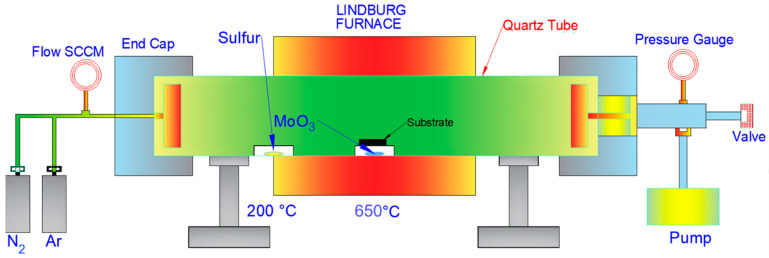
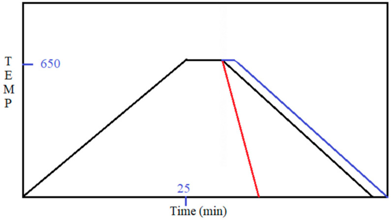
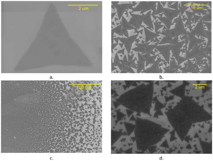
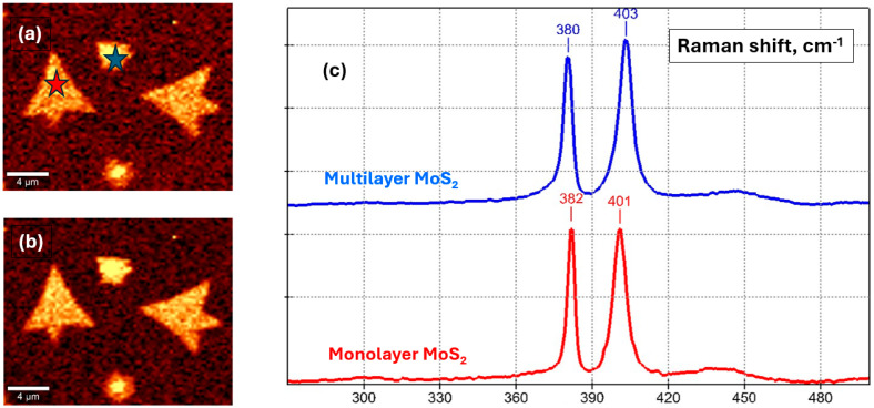
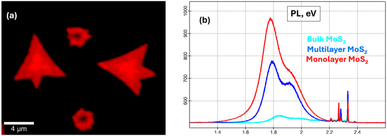
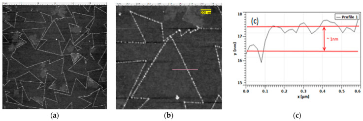
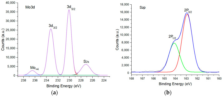
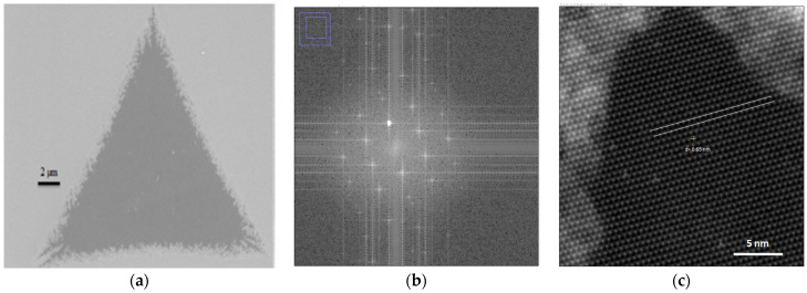
Molybdenum disulfide (MoS2) transistors are a promising alternative for the semiconductor industry due to their large on/off current ratio (>1010), immunity to short-channel effects, and unique switching characteristics. MoS2 has drawn considerable interest due to its intriguing electrical, optical, sensing, and catalytic properties. Monolayer MoS2 is a semiconducting material with a direct band gap of ~1.9 eV, which can be tuned. Commercially, the aim of synthesizing a novel material is to grow high-quality samples over a large area and at a low cost. Although chemical vapor deposition (CVD) growth techniques are associated with a low-cost pathway and large-area material growth, a drawback concerns meeting the high crystalline quality required for nanoelectronic and optoelectronic applications. This research presents a lower-temperature CVD for the repeatable synthesis of large-size mono- or few-layer MoS2 using the direct vapor phase sulfurization of MoO3. The samples grown on Si/SiO2 substrates demonstrate a uniform single-crystalline quality in Raman spectroscopy, photoluminescence (PL), scanning electron microscopy (SEM), atomic force microscopy (AFM), X-ray photoelectron spectroscopy (XPS), and scanning transmission electron microscopy. These characterization techniques were targeted to confirm the uniform thickness, stoichiometry, and lattice spacing of the MoS2 layers. The MoS2 crystals were deposited over the entire surface of the sample substrate. With a detailed discussion of the CVD setup and an explanation of the process parameters that influence nucleation and growth, this work opens a new platform for the repeatable synthesis of highly crystalline mono- or few-layer MoS2 suitable for optoelectronic application.
Keywords: MoS2; Raman spectroscopy; X-ray photoelectron spectroscopy; atomic force microscopy; chemical vapor deposition; monolayer; photoluminescence; scanning electron microscopy; scanning tunneling electron microscopy.
Conflict of interest statement
The authors declare no conflict of interest.
Figures
Similar articles
-
NaCl-Assisted Temperature-Dependent Controllable Growth of Large-Area MoS2 Crystals Using Confined-Space CVD.ACS Omega. 2022 Aug 22;7(34):30074-30086. doi: 10.1021/acsomega.2c03108. eCollection 2022 Aug 30. ACS Omega. 2022. PMID: 36061644 Free PMC article.
-
Application-Oriented Growth of a Molybdenum Disulfide (MoS2) Single Layer by Means of Parametrically Optimized Chemical Vapor Deposition.Materials (Basel). 2020 Jun 20;13(12):2786. doi: 10.3390/ma13122786. Materials (Basel). 2020. PMID: 32575719 Free PMC article.
-
Ambient Pressure Chemical Vapor Deposition of Flat and Vertically Aligned MoS2 Nanosheets.Nanomaterials (Basel). 2022 Mar 16;12(6):973. doi: 10.3390/nano12060973. Nanomaterials (Basel). 2022. PMID: 35335786 Free PMC article.
-
Influence of stoichiometry on the optical and electrical properties of chemical vapor deposition derived MoS2.ACS Nano. 2014 Oct 28;8(10):10551-8. doi: 10.1021/nn503988x. Epub 2014 Sep 22. ACS Nano. 2014. PMID: 25223821 Free PMC article.
-
Instrumental Techniques for Characterization of Molybdenum Disulphide Nanostructures.J Anal Methods Chem. 2020 Dec 16;2020:8896698. doi: 10.1155/2020/8896698. eCollection 2020. J Anal Methods Chem. 2020. PMID: 33381353 Free PMC article. Review.
Cited by
-
Nonlinear Static Bending and Forced Vibrations of Single-Layer MoS2 with Thermal Stress.Materials (Basel). 2024 Apr 10;17(8):1735. doi: 10.3390/ma17081735. Materials (Basel). 2024. PMID: 38673092 Free PMC article.
References
-
- Li H., Zhang Q., Yap C.C.R., Tay B.K., Edwin T.H.T., Olivier A., Baillargeat D. From bulk to monolayer MoS2: Evolution of Raman scattering. Adv. Funct. Mater. 2012;22:1385–1390. doi: 10.1002/adfm.201102111. - DOI
Grants and funding
LinkOut - more resources
Full Text Sources
Miscellaneous
