. 2023 Oct 12;13(1):17278.
doi: 10.1038/s41598-023-43702-w.

Influence of Bi doping on the electronic structure of (Ga,Mn)As epitaxial layers

Affiliations

Influence of Bi doping on the electronic structure of (Ga,Mn)As epitaxial layers

Oksana Yastrubchak et al. Sci Rep. .

Abstract

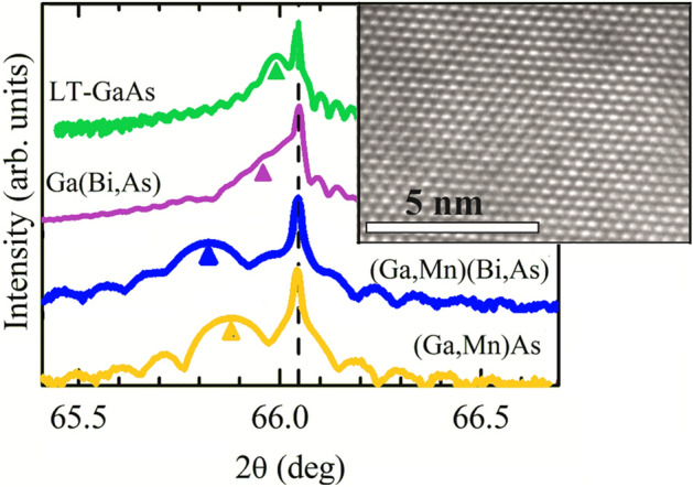
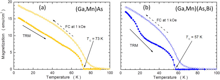
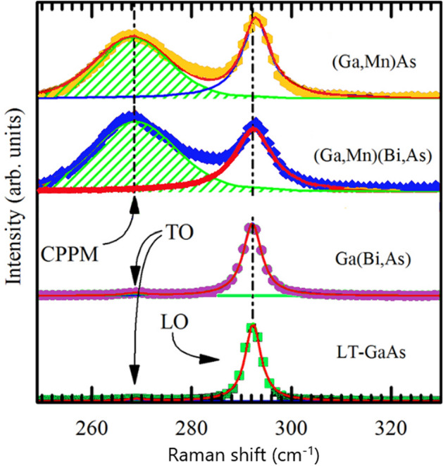
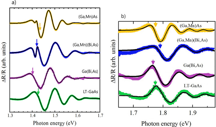
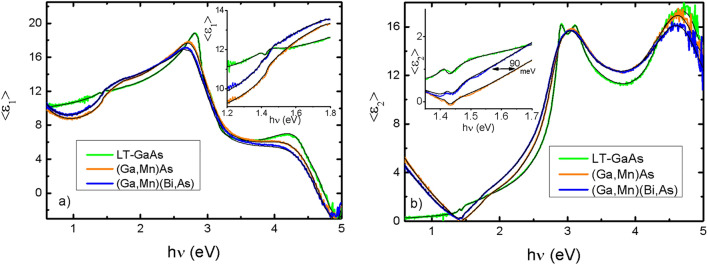
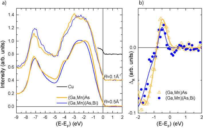
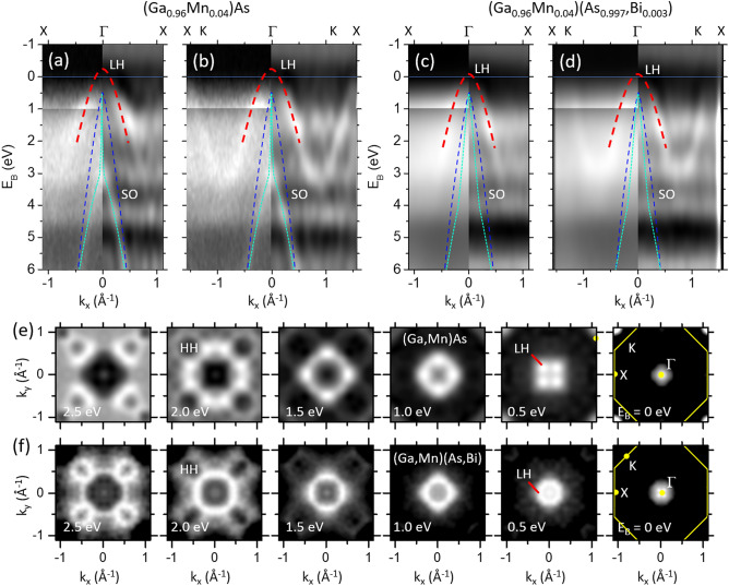
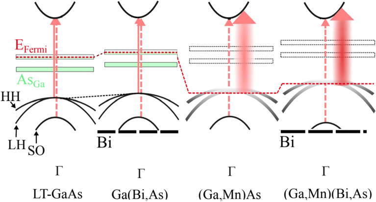
The influence of the addition of Bi to the dilute ferromagnetic semiconductor (Ga,Mn)As on its electronic structure as well as on its magnetic and structural properties has been studied. Epitaxial (Ga,Mn)(Bi,As) layers of high structural perfection have been grown using low-temperature molecular-beam epitaxy. Post-growth annealing of the samples improves their structural and magnetic properties and increases the hole concentration in the layers. Hard X-ray angle-resolved photoemission spectroscopy reveals a strongly dispersing band in the Mn-doped layers, which crosses the Fermi energy and is caused by the high concentration of Mn-induced itinerant holes located in the valence band. An increased density of states near the Fermi level is attributed to additional localized Mn states. In addition to a decrease in the chemical potential with increasing Mn doping, we find significant changes in the valence band caused by the incorporation of a small atomic fraction of Bi atoms. The spin-orbit split-off band is shifted to higher binding energies, which is inconsistent with the impurity band model of the band structure in (Ga,Mn)As. Spectroscopic ellipsometry and modulation photoreflectance spectroscopy results confirm the valence band modifications in the investigated layers.


Conflict of interest statement

The authors declare no competing interests.

Figures

Figure 1
Figure 1
High-resolution X-ray diffraction patterns: 2θ/ω scans for 004 Bragg reflections for the LT-GaAs and Ga(Bi,As) layers and annealed (Ga,Mn)(Bi,As) and (Ga,Mn)As layers epitaxially grown on the (001) semi-insulating GaAs substrate. The narrow line corresponds to the reflection from the GaAs substrate. The broader structures at lower angles, indicated by the arrows, are reflections from the deposited layers. The results have been vertically offset for clarity. The inset shows a high-resolution TEM cross-sectional image of the (Ga,Mn)(Bi,As) epitaxial layer.
Figure 2
Figure 2
Temperature dependent magnetization of the annealed (Ga,Mn)As (a) and (Ga,Mn)(Bi,As) (b) layers measured with SQUID magnetometry. FC denotes the field cooling of the layers under magnetic field of 1 kOe applied along the [100] in-plane crystallographic direction and TRM denotes the thermoremnant magnetization measured during warming up the samples under zero magnetic field. The positions of Curie temperatures, TC, are indicated with arrows.
Figure 3
Figure 3
μ-Raman spectra recorded in the backscattering configuration at room temperature for the LT-GaAs and Ga(Bi,As) layers, as well as the annealed (Ga,Mn)As and (Ga,Mn)(Bi,As) layers. The spectra have been vertically offset for clarity. The dashed line indicates the position of the Raman LO-phonon line for the reference LT-GaAs layer. The positions of the TO-phonon lines for the LT-GaAs and Ga(Bi,As) reference layers are indicated by arrows. The hatched areas represent the CPPM peaks resulting from the full line-shape analysis of the spectra for the Mn-doped layers.
Figure 4
Figure 4
Normalized photoreflectence spectra for the 150 nm thick as-grown LT-GaAs and Ga(Bi,As) layers and the 100 nm thick annealed (Ga,Mn)As and (Ga,Mn)(Bi,As) layers with 4% Mn and 0.3% Bi contents, epitaxially grown on GaAs substrate, (symbols) with the fits to the experimental data by full line-shape analysis of the spectra for the lower (a) and higher (b) range of photon energy. The arrows indicate the E0 (a) and E0 + ∆0 (b) transition energies for each layer obtained from the full line-shape analysis. The spectra have been vertically offset for clarity. For thinner (Ga,Mn)As and (Ga,Mn) (Bi,As) layers, an additional feature at photon energy of about 1.41 eV, corresponding to the layer-substrate interface, is observed.
Figure 5
Figure 5
Spectral dependencies of pseudo dielectric function < ε1 > and < ε2 > for LT-GaAs, (Ga,Mn)As and (Ga,Mn)(Bi,As) samples and corresponding fits. Insets show near band gap region a larger scale.
Figure 6
Figure 6
(a) Photoelectron spectra for annealed (Ga,Mn)As and (Ga,Mn)(Bi,As) layers integrated in momentum space over a circle centered at the Γ-point with radius R. The intensity is normalized at EB = 2 eV. The Fermi edge for the Cu-carrier is shown as reference for the binding-energy scale. The spectra have been vertically offset for clarity. (b) Normalized difference, ΔR = I(R2) − I(R1), of photoelectron intensity averaged over R1 = 0.5 Å−1 and R2 = 0.1 Å−1, respectively. Full lines represent fits with two Gaussian functions to model the onset of the spin–orbit split off band at the Γ-point.
Figure 7
Figure 7
(a − d) Band dispersion plots EB versus k|| along the Γ-X (a, c) and Γ-K direction (b, d) for the annealed (Ga,Mn)As (a,b) and (Ga,Mn)(Bi,As) (c,d) layers. The photoemission intensity distribution is displayed with enhanced contrast for EB < 1 eV (left panels). Laplacian derivative plots are shown on the right halves of panels (a − d) to increase the band contrast. Parabolas indicate the LH (red) and SO (green) bands. For comparison, parabolas (blue) with maxima at 0.5 eV and parallel momentum of 0.4 Å−1 at EB = 6 eV indicate the dispersion expected from the theory (see e.g.). (e,f) Series of kx – ky maps at the indicated binding energies EB for (Ga,Mn)As (e) and (Ga,Mn)(Bi,As) (f). The Brillouin zone is indicated in the rightmost panels (yellow lines).
Figure 8
Figure 8
Schematic energy band diagrams for the LT-GaAs, Ga(Bi,As), (Ga,Mn)As and (Ga,Mn)(Bi,As) layers in the vicinity of Γ point of the Brillouin zone. Arrows indicate electronic transitions from the valence band (E0) and spin–orbit split off band (E0 + Δ0) to the conduction band. The Fermi level is denoted by the red dashed line and HH, LH and SO parabolas denote the heavy-, light-hole and spin–orbit split off subbands, respectively. Thick dashed line denotes the Bi-induced level in the valence band.

References

    1. Dietl T. A ten-year perspective on dilute magnetic semiconductors and oxides. Nat. Mater. 2010;9(12):965–974. doi: 10.1038/nmat2898. - DOI - PubMed
    1. Medjanik K, Fedchenko O, Yastrubchak O, Sadowski J, Sawicki M, Gluba L, Vasilyev D, Babenkov S, Chernov S, Winkelmann A, Elmers HJ, Schönhense G. Site-specific atomic order and band structure tailoring in the diluted magnetic semiconductor (In, Ga, Mn)As. Phys. Rev. B. 2021;103:075107. doi: 10.1103/PhysRevB.103.075107. - DOI
    1. Yastrubchak O, Sadowski J, Gluba L, Domagala JZ, Rawski M, Żuk J, Kulik M, Andrearczyk T, Wosinski T. Ferromagnetism and the electronic band structure in (Ga, Mn)(Bi, As) epitaxial layers. Appl. Phys. Lett. 2014;105(7):072402. doi: 10.1063/1.4893381. - DOI
    1. Yastrubchak O, Riney L, Powers W, Tataryn N, Mamykin S, Kondratenko O, Romanyuk V, Borkovska L, Kolomys O, Khomenkova L, Wang J, Liu X, Furdyna JK, Assaf BA. Band engineering of magnetic semiconductors by phosphorus doping. IEEE Trans. Magn. 2023 doi: 10.1109/TMAG.2023.3287730. - DOI
    1. Tataryn N, Gluba L, Yastrubchak O, Sadowski J, Adreanczyk T, Mamykin S, Sawicki M, Wosinski T. Valence band dispersion in Bi doped (Ga, Mn)As epitaxial layers. IEEE Trans. Magn. 2023 doi: 10.1109/TMAG.2023.3284538. - DOI