Review
. 2023 Sep 22;26(10):107946.
doi: 10.1016/j.isci.2023.107946. eCollection 2023 Oct 20.

Roadmap for phase change materials in photonics and beyond

Affiliations
Review

Roadmap for phase change materials in photonics and beyond

Patinharekandy Prabhathan et al. iScience. .

Erratum in

  • Erratum: Roadmap for phase change materials in photonics and beyond.
    Prabhathan P, Sreekanth KV, Teng J, Ko JH, Yoo YJ, Jeong HH, Lee Y, Zhang S, Cao T, Popescu CC, Mills B, Gu T, Fang Z, Chen R, Tong H, Wang Y, He Q, Lu Y, Liu Z, Yu H, Mandal A, Cui Y, Ansari AS, Bhingardive V, Kang M, Lai CK, Merklein M, Müller MJ, Song YM, Tian Z, Hu J, Losurdo M, Majumdar A, Miao X, Chen X, Gholipour B, Richardson KA, Eggleton BJ, Sharda K, Wuttig M, Singh R. Prabhathan P, et al. iScience. 2023 Nov 6;26(12):108396. doi: 10.1016/j.isci.2023.108396. eCollection 2023 Dec 15. iScience. 2023. PMID: 38025789 Free PMC article.

Abstract

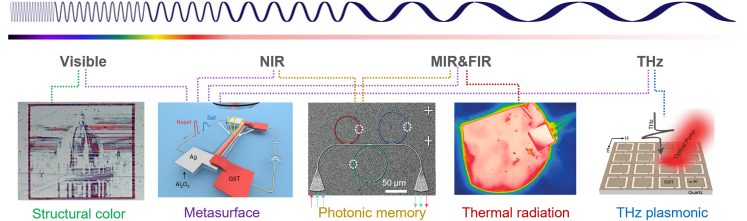
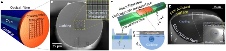
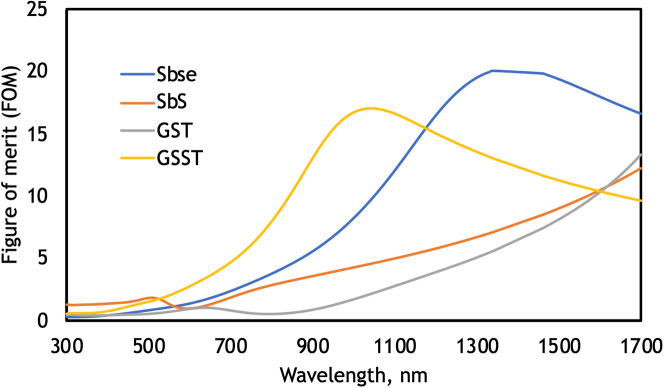
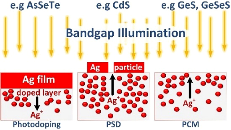
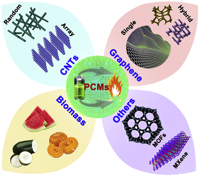
Phase Change Materials (PCMs) have demonstrated tremendous potential as a platform for achieving diverse functionalities in active and reconfigurable micro-nanophotonic devices across the electromagnetic spectrum, ranging from terahertz to visible frequencies. This comprehensive roadmap reviews the material and device aspects of PCMs, and their diverse applications in active and reconfigurable micro-nanophotonic devices across the electromagnetic spectrum. It discusses various device configurations and optimization techniques, including deep learning-based metasurface design. The integration of PCMs with Photonic Integrated Circuits and advanced electric-driven PCMs are explored. PCMs hold great promise for multifunctional device development, including applications in non-volatile memory, optical data storage, photonics, energy harvesting, biomedical technology, neuromorphic computing, thermal management, and flexible electronics.

Keywords: Applied physics; Materials application; Physics.


Conflict of interest statement

The authors declare no competing interests.

Figures

Figure 1
Figure 1
Refractive index variation of PCMs from visible to terahertz The refractive indices are obtained from the literatures Adapted from.,,,,,,,,,,
Figure 2
Figure 2
Applications of tunable photonics with PCMs Reproduced with permission from.,,,,,
Figure 3
Figure 3
2D map classifying chemical bonding in solids The map is spanned by the number of electrons shared between adjacent atoms and the electron transfer renormalized by the formal oxidation state. Different colors characterize different material properties and have been related to different types of bonds. Adapted from.,, Filled and open symbols represent thermodynamically stable and metastable phases. The red – black line describes the transition from ideal covalent bonds to perfect ionic bonds. The dashed green line indicates metavalently bonded solids with perfect octahedral arrangement like cubic Sb, AgSbTe2 and PbS, while distorted octahedrally coordinated structures are situated above it, characterized by a larger number of electrons shared. Map adapted from.
Figure 4
Figure 4
Minimum crystallization time and its dependence on the chemical bond indicators introduced in Figure 3 Sb2Se3 represents a covalently bonded material, while typical phase change materials like Ge2Sb2Te5 or GeTe are metavalently bonded. Adapted from.,
Figure 5
Figure 5
Various PCM platforms explored for demonstrating tunable nanophotonic applications in the UV to THz spectral range
Figure 6
Figure 6
Sb2Te3 based metasurfaces and optical properties (A) Optical microscope image of fabricated microheater integrated Sb2Te3/Si PCM device. (B) Scanning electron microscope image of fabricated Sb2Te3 based metasurfaces. (C and D) Measured reflectance spectra of 2D grating holes with applied current (c) hole diameter = 120 nm and period = 200 nm and (d) hole diameter = 80 nm and period = 150 nm. Adapted from.,,
Figure 7
Figure 7
Roadmap for THz reconfigurable photonics with PCM The metasurface tree shows developments and future of THz reconfigurable metasurface research. The ripe fruits: the research have been reported and realized experimentally. The unripe fruits: the futuristic research that are on the roadmap.
Figure 8
Figure 8
Optical properties of Sb2S3 (A) Variation of the optical bandgap of Sb2S3 as a function of layered-3D polymorph crystalline-to-crystalline transition occurring by stress/pressure variation. (B and C) 532 nm laser writing of the amorphous-to-crystalline transition, as confirmed by the Raman spectra in (c).
Figure 9
Figure 9
Switchable modulators and metasurfaces (A) The design of MZI phase modulator equipped with PCM cell atop one of the arms in two configurations: patterned cells and unpatterned cell. (B) Microscope image of the Sb2S3-based MZI device on InP waveguide, with the colorized-SEM image of Sb2S3 patterned on the InP waveguide. Adapted from. (C) Scheme of the resonant Sb2S3-LN metasurface with a pair of Au electrodes, with the reflection spectra showing the tunability and the shift of the plasmon resonance with different gate voltage from 0 V to 200 V. Adapted from.
Figure 10
Figure 10
(top) A broadband 2×2 silicon photonic switch based on GST and doped silicon PIN heaters Adapted from Chen, Rui et al. “Broadband Nonvolatile Electrically Controlled Programmable Units in Silicon Photonics.” ACS Photonics 9.6 (2022): 2142–2150. (bottom) A low-loss phase shifter based on Sb2Se3 controlled by a graphene heater. Adapted from Fang, Zhuoran et al. “Ultra-low-energy programmable non-volatile silicon photonics based on phase-change materials with graphene heaters.” Nature Nanotechnology 17.8 (2022): 842–848.
Figure 11
Figure 11
Fully integrated and reconfigurable microwave or optical signal processor (A) The proposed architecture incorporating tunable bandpass filtering or non-volatile computing, microwave photonics signal processing, linear isolators and some active on-chip components such as lasers, EO-modulator, arrayed waveguide grating (AWG), true time delay (TTD) unit, Erbium doped amplifiers, and photodetectors, Adapted from. (B) Silicon PIN diode heaters, Adapted from. (C) Graphene microheater, Adapted from,, licensed under a Creative Commons Attribution (CC BY) license. (D) Chalcogenide PCM coated waveguide, Adapted from. (E) Nonlinear SBS waveguide, Adapted from. (F) Vertical taper technology for off-chip coupling, Adapted from. Figures and insets adapted from the ref. ,,,,,,.
Figure 12
Figure 12
Operation principle of the proposed phase change all-optical switch The phase change materials thin film is sandwiched by ZnS/SiO2 and SiO2. Laser pulses control the phase transition between amorphous and crystalline states, which show dramatic refractive index difference. The resonance wavelength can be finely tuned by changing dimeter D and period P.
Figure 13
Figure 13
Integration and packaging of phase change metasurfaces (A–D) Shows schematic and scanning electron microscopy of metadevices fabricated on (a, b) tip and (c, d) side of optical fiber, Adapted from.,
Figure 14
Figure 14
Visible and near infrared dispersion of figure of merit defined for a reconfigurable phase change nanophotonic medium (FOM =naΔnkc), where na is refractive index of amorphous phase and kc extinction coefficient of the lossy crystalline phase
Figure 15
Figure 15
Comparison of different forms of photo-ionic movement possible in various chalcogenides It illustrates a comparison of the Ag photodoping, Photo-induced surface deposition (PSD) and photo-induced chemical modification (PCM) phenomena.
Figure 16
Figure 16
Main conductive supporting scaffolds for electric-driven composite PCMs Adapted with permission from.,

References

    1. Ko J.H., Yoo Y.J., Lee Y., Jeong H.-H., Song Y.M. A review of tunable photonics: Optically active materials and applications from visible to terahertz. iScience. 2022 - PMC - PubMed
    1. Delaney M., Zeimpekis I., Lawson D., Hewak D.W., Muskens O.L. A New Family of Ultralow Loss Reversible Phase-Change Materials for Photonic Integrated Circuits: Sb2S3 and Sb2Se3. Adv. Funct. Mater. 2020;30
    1. Derkaoui I., Khenfouch M., Benkhali M., Rezzouk A. Journal of Physics: Conference Series, IOP Publishing. 2019. VO2 thin films for smart windows: Numerical study of the optical properties and performance improvement.
    1. Julian M.N., Williams C., Borg S., Bartram S., Kim H.J. Reversible optical tuning of GeSbTe phase-change metasurface spectral filters for mid-wave infrared imaging. Optica. 2020;7:746–754. - PMC - PubMed
    1. Liu H., Dong W., Wang H., Lu L., Ruan Q., Tan Y.S., Simpson R.E., Yang J.K.W. Rewritable color nanoprints in antimony trisulfide films. Sci. Adv. 2020;6 - PMC - PubMed

LinkOut - more resources