. 2023 Oct 20;9(42):eadj5379.
doi: 10.1126/sciadv.adj5379. Epub 2023 Oct 20.

Remote epitaxial interaction through graphene

Affiliations

Remote epitaxial interaction through graphene

Celesta S Chang et al. Sci Adv. .

Abstract

The concept of remote epitaxy involves a two-dimensional van der Waals layer covering the substrate surface, which still enable adatoms to follow the atomic motif of the underlying substrate. The mode of growth must be carefully defined as defects, e.g., pinholes, in two-dimensional materials can allow direct epitaxy from the substrate, which, in combination with lateral epitaxial overgrowth, could also form an epilayer. Here, we show several unique cases that can only be observed for remote epitaxy, distinguishable from other two-dimensional material-based epitaxy mechanisms. We first grow BaTiO3 on patterned graphene to establish a condition for minimizing epitaxial lateral overgrowth. By observing entire nanometer-scale nuclei grown aligned to the substrate on pinhole-free graphene confirmed by high-resolution scanning transmission electron microscopy, we visually confirm that remote epitaxy is operative at the atomic scale. Macroscopically, we also show variations in the density of GaN microcrystal arrays that depend on the ionicity of substrates and the number of graphene layers.


Figures

Fig. 1.
Fig. 1.. Schematics of three different mechanisms of growth upon an intervening vdW layer nominally covering a substrate surface.
3D schematics show the growth mechanism of (A) remote, (B) quasi-vdW, and (C) pinhole-based epitaxy methods. vdW epitaxy refers to epitaxial growth on a dangling bond–free substrate via weak vdW interaction between grown materials and the substrate. Therefore, (B) is a quasi-vdW epitaxy where conventional bulk material with initial dangling bonds (usually 3D materials) is grown on a vdW substrate, which corresponds to the examples shown in our study. The grown epilayer exhibits incommensurate in-plane lattices, and the alignment follows the underlying vdW surface as shown. Cross-sectional view depicted below highlights the differences among these mechanisms. (D) Summary of various materials showing the effect of polarity on remote epitaxy. Nonpolar substrates such as Si and Ge lead to polycrystalline epilayers, while polar GaAs can induce remote epitaxy of a single-crystalline GaAs film. The polarity of the film also matters, as shown by polycrystalline Ge grown on graphene-covered polar GaAs substrate.
Fig. 2.
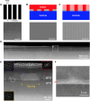
Fig. 2.. Oxide growth on patterned graphene.
(A) Graphene is patterned using electron-beam lithography (EBL), with width and period as defined in the schematics. An example of patterned graphene on a STO substrate with dark (graphene) and bright stripes (openings) is shown in the scanning electron microscopy (SEM) image. Expectation and actual results for epilayer growth of materials with different diffusion lengths are shown in (B) and (C). (B) GaAs grown on patterned graphene with width and period of 100 and 200 nm, respectively, shows a smooth surface as a result of lateral overgrowth of nucleation sites from the openings. (C) Plane-view SEM image of BTO grown on patterned graphene of width 200 nm and period of 800 nm shows a different surface morphology correlated to the pattern. Bare substrate region leads to smooth surface while multigraphene region results in a rough surface of BTO. (D and E) Cross-sectional high-angle annular dark-field imaging (HAADF)–scanning transmission electron microscopy (STEM) image of BTO grown on patterned graphene with a width of 100- and 800-nm period shows crystallinity of each region more clearly. The distinguishable contrast reveals single (bright)– and poly (dark)–crystalline region. Insets in (E) show selected-area electron diffraction (SAED) patterns for each region confirming its crystallinity. (F) The white-boxed region in (E) is enlarged to show trilayer graphene under polycrystalline domains. A set of three red lines indicating each graphene layer on the left serves as a guide to the eye. Scale bars, (A) to (C), 2 μm.
Fig. 3.
Fig. 3.. TEM images of pinhole-based epitaxy and remote epitaxy of BTO grown on gr/STO.
(A) Example of an area showing direct growth through pinholes. Direct growth regions are denoted with red arrows. They do not show lateral growth leading to single-crystalline film aligned to the substrate; instead, we can observe domains with in-plane rotation. The schematic in the right shows simplified domains to aid understanding. (B) The schematic depicts the encapsulated nuclei within the sampled TEM specimen. TEM images are acquired perpendicular to the cross-section, where the electron beam direction is denoted by a white cross. (C and D) Simultaneously taken HAADF- and ABF-STEM images of remote-epitaxially formed island without any pinholes, respectively, are shown. The atomic alignments of the island follow the bottom substrate lattice. Bilayer graphene without pinholes can be observed from (D).
Fig. 4.
Fig. 4.. Influence of graphene thickness on remote epitaxy of GaN μCs.
Plane-view SEM images of remote epitaxial GaN μCs grown on (A) SLG-, (B) BLG-, and (C) MLG-grown SiC substrates. (D) Plot of growth density of μCs as a function of number of graphene layers. SEM images of (E) bottom side of exfoliated PI-encapsulated GaN μCs and (F) substrate surface after the exfoliation process.
Fig. 5.
Fig. 5.. Influence of substrate with different ionicity and growth temperatures on remote epitaxy GaN μCs.
Plane-view SEM images of GaN μCs grown on graphene-coated (A) Al2O3 and (B) N-polar GaN substrates under growth temperature conditions of 900°, 950°, and 1000°C. Orange arrows indicate the in-plane orientation of {1010} sidewall facets of μCs. (C) Comparison of growth density of GaN μCs grown on graphene/Al2O3 (red columns) and graphene/GaN substrates (blue columns) at 900°, 950°, and 1000°C. The growth density of μCs grown on graphene/Al2O3 at 900°, 950°, and 1000°C were (5.7 ± 0.5) × 106, (3.7 ± 0.6) × 106, and (1.4 ± 0.1) × 106 cm−2, respectively. The growth density of μCs grown on graphene/GaN at 900°, 950°, and 1000°C were (3.8 ± 0.8) × 106, (1.6 ± 0.2) × 106, and (1.1 ± 0.1) × 106 cm−2, respectively.

References

    1. Y. Kim, S. S. Cruz, K. Lee, B. O. Alawode, C. Choi, Y. Song, J. M. Johnson, C. Heidelberger, W. Kong, S. Choi, K. Qiao, I. Almansouri, E. A. Fitzgerald, J. Kong, A. M. Kolpak, J. Hwang, J. Kim, Remote epitaxy through graphene enables two-dimensional material-based layer transfer. Nature 544, 340–343 (2017). - PubMed
    1. W. Kong, H. Li, K. Qiao, Y. Kim, K. Lee, Y. Nie, D. Lee, T. Osadchy, R. J. Molnar, D. K. Gaskill, R. L. Myers-Ward, K. M. Daniels, Y. Zhang, S. Sundram, Y. Yu, S.-H. Bae, S. Rajan, Y. Shao-Horn, K. Cho, A. Ougazzaden, J. C. Grossman, J. Kim, Polarity governs atomic interaction through two-dimensional materials. Nat. Mater. 17, 999–1004 (2018). - PubMed
    1. H. Kum, D. Lee, W. Kong, H. Kim, Y. Park, Y. Kim, Y. Baek, S.-H. Bae, K. Lee, J. Kim, Epitaxial growth and layer-transfer techniques for heterogeneous integration of materials for electronic and photonic devices. Nat. Electron. 2, 439–450 (2019).
    1. S.-H. Bae, K. Lu, Y. Han, S. Kim, K. Qiao, C. Choi, Y. Nie, H. Kim, H. S. Kum, P. Chen, W. Kong, B.-S. Kang, C. Kim, J. Lee, Y. Baek, J. Shim, J. Park, M. Joo, D. A. Muller, K. Lee, J. Kim, Graphene-assisted spontaneous relaxation towards dislocation-free heteroepitaxy. Nat. Nanotechnol. 15, 272–276 (2020). - PubMed
    1. H. Kim, K. Lu, Y. Liu, H. S. Kum, K. S. Kim, K. Qiao, S.-H. Bae, S. Lee, Y. J. Ji, K. H. Kim, H. Paik, S. Xie, H. Shin, C. Choi, J. H. Lee, C. Dong, J. A. Robinson, J.-H. Lee, J.-H. Ahn, G. Y. Yeom, D. G. Schlom, J. Kim, Impact of 2D–3D heterointerface on remote epitaxial interaction through graphene. ACS Nano 15, 10587–10596 (2021). - PubMed

LinkOut - more resources