. 2023 Nov 1;13(1):18845.
doi: 10.1038/s41598-023-44232-1.

Nano-scale charge trapping memory based on two-dimensional conjugated microporous polymer

Affiliations

Nano-scale charge trapping memory based on two-dimensional conjugated microporous polymer

Ayman Rezk et al. Sci Rep. .

Abstract

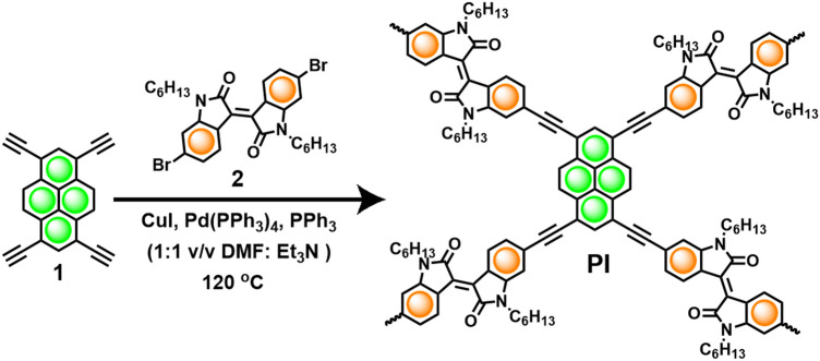
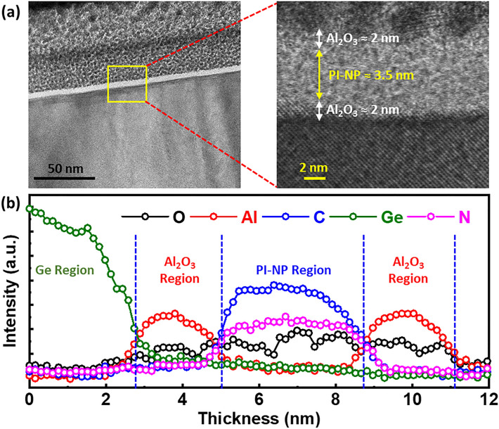
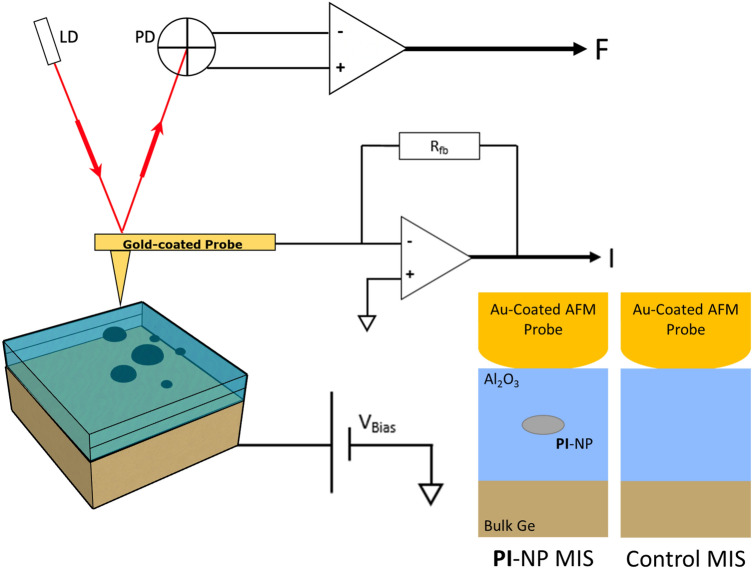
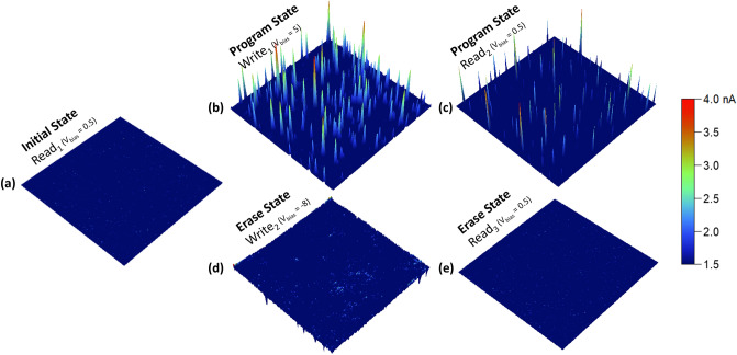
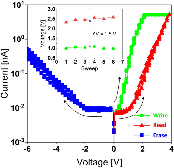
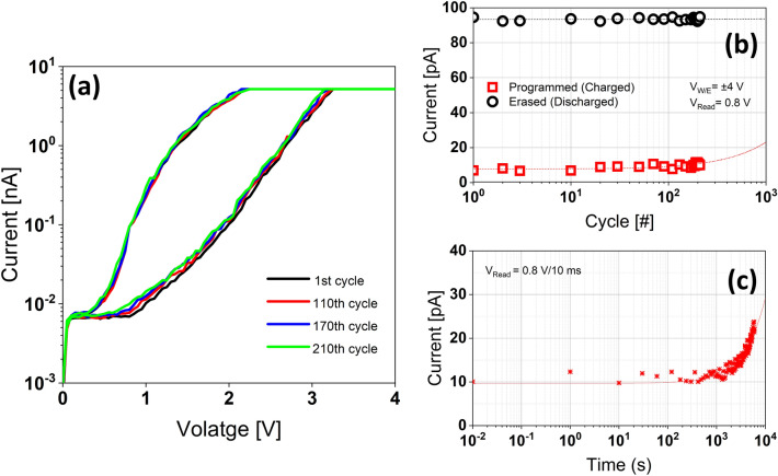
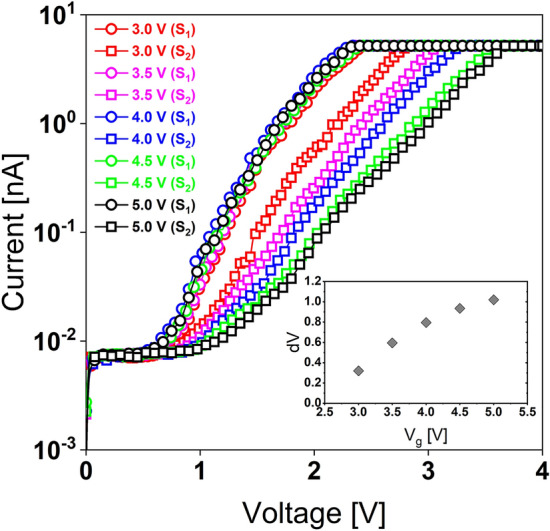
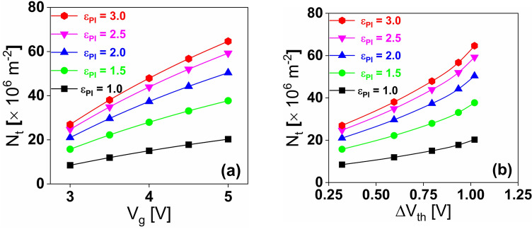
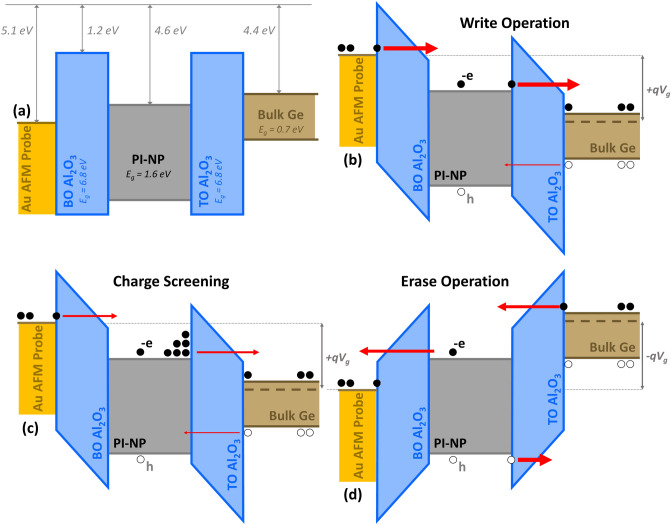
There is a growing interest in new semiconductor nanostructures for future high-density high-performance flexible electronic devices. Two-dimensional conjugated microporous polymers (2D-CMPs) are promising candidates because of their inherent optoelectronic properties. Here, we are reporting a novel donor-acceptor type 2D-CMP based on Pyrene and Isoindigo (PI) for a potential nano-scale charge-trapping memory application. We exfoliated the PI polymer into ~ 2.5 nm thick nanoparticles (NPs) and fabricated a Metal-Insulator-Semiconductor (MIS) device with PI-NPs embedded in the insulator. Conductive AFM (cAFM) is used to examine the confinement mechanism as well as the local charge injection process, where ultrathin high-κ alumina supplied the energy barrier for confining the charge carrier transport. We have achieved a reproducible on-and-off state and a wide memory window (ΔV) of 1.5 V at a relatively small reading current. The device displays a low operation voltage (V < 1 V), with good retention (104 s), and endurance (103 cycles). Furthermore, a theoretical analysis is developed to affirm the measured charge carriers' transport and entrapment mechanisms through and within the fabricated MIS structures. The PI-NPs act as a nanoscale floating gate in the MIS-based memory with deep trapping sites for the charged carriers. Moreover, our results demonstrate that the synthesized 2D-CMP can be promising for future low-power high-density memory applications.


Conflict of interest statement

The authors declare no competing interests.

Figures

Figure 1
Figure 1
Synthetic approach for the rationally designed Pyrene-Isoindigo 2D-CMP (PI).
Figure 2
Figure 2
A schematic of the fabricated MIS structure with the embedded PI–NPs, showing the process flow.
Figure 3
Figure 3
(a) Topography AFM scans in AC mode of the surface with the spin-coated PI–NPs on top of the Al2O3 BO along with the associated. (b) AFM scan of the BO before spin-coating and the RMS roughness. (c) Height and (d) mean radius distribution of PI–NPs.
Figure 4
Figure 4
(a) Cross-sectional transmission electron microscopy (XTEM) image of the Pt-coated structure, showing the fabricated MIS stack with the embedded PI–NPs. (b) EELS compositional mapping of the stack.
Figure 5
Figure 5
(a) The circuit of surface mapping and electrical probing of a single PI–NP using conductive-AFM. Inset shows a cross-section view of the probed MIS stack with and without the PI–NP.
Figure 6
Figure 6
2.5 × 2.5 µm2 current maps of the (a) initial, (b) write, (c) read, (d) erase and (e) read scans.
Figure 7
Figure 7
I-V characteristics for two successive sweeps at points A and B of the (a) MISA stack, as well as for points C and D of the (b) MISB stack.
Figure 8
Figure 8
Six sets of successive write (green), read (red), erase (blue) IV sweeps. Inset highlights a memory window of 1.46 V at 200 pA.
Figure 9
Figure 9
(a) IV sweeps of MISA structure throughout the endurance test at VW/E =  ± 4 V after 1, 110, 170 and 210 cycles. (b) Endurance characteristics for 210 W/E cycles extracted at VRead = 0.8 V from IV sweeps. (c) Retention characteristics up to 104 s at VW/E =  ± 4 V and VRead = 0.8 V.
Figure 10
Figure 10
IV sweeps at different voltage biases. Inset shows the memory window vs bias voltage.
Figure 11
Figure 11
Capacitance at different dielectric constant values of PI.
Figure 12
Figure 12
Variation in charge trap density with (a) applied gate voltage (Vg) and (b) change in threshold voltage (ΔVth) for different dielectric constants of PI.
Figure 13
Figure 13
(a) Variation in Electric field across the tunneling oxide with gate voltage for the different dielectric constant of PI. (b) Variation in natural log of (ΔVth/E) with (1/E) across the tunneling oxide for εPI = 3.0.
Figure 14
Figure 14
The energy band diagram for (a) flat band state, (b) charge injection during write operation, (c) charge screening, and (d) charge ejection during erase operation within the embedded PI–NP when probed using a conductive AFM Tip. The varying thickness of the red arrows symbolizes the magnitude of tunneling current.

References

    1. Lee J-SM, Cooper AI. Advances in conjugated microporous polymers. Chem. Rev. 2020;120(4):2171–2214. doi: 10.1021/acs.chemrev.9b00399. - DOI - PMC - PubMed
    1. Chaoui N, Trunk M, Dawson R, Schmidt J, Thomas A. Trends and challenges for microporous polymers. Chem. Soc. Rev. 2017;46(11):3302–3321. doi: 10.1039/C7CS00071E. - DOI - PubMed
    1. Geng K, Arumugam V, Xu H, Gao Y, Jiang D. Covalent organic frameworks: Polymer chemistry and functional design. Prog. Polym. Sci. 2020;108:101288. doi: 10.1016/j.progpolymsci.2020.101288. - DOI
    1. Martínez-Abadía M, Mateo-Alonso A. Structural approaches to control interlayer interactions in 2D covalent organic frameworks. Adv. Mater. 2020;32(40):2002366. doi: 10.1002/adma.202002366. - DOI - PubMed
    1. Evans AM, Strauss MJ, Corcos AR, Hirani Z, Ji W, Hamachi LS, Aguilar-Enriquez X, Chavez AD, Smith BJ, Dichtel WR. Two-dimensional polymers and polymerizations. Chem. Rev. 2021;122(1):442–564. doi: 10.1021/acs.chemrev.0c01184. - DOI - PubMed