. 2023 Nov 20;14(1):7550.
doi: 10.1038/s41467-023-42256-9.

Direct imaging of electron density with a scanning transmission electron microscope

Affiliations

Direct imaging of electron density with a scanning transmission electron microscope

Ondrej Dyck et al. Nat Commun. .

Abstract

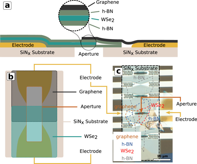
Recent studies of secondary electron (SE) emission in scanning transmission electron microscopes suggest that material's properties such as electrical conductivity, connectivity, and work function can be probed with atomic scale resolution using a technique known as secondary electron e-beam-induced current (SEEBIC). Here, we apply the SEEBIC imaging technique to a stacked 2D heterostructure device to reveal the spatially resolved electron density of an encapsulated WSe2 layer. We find that the double Se lattice site shows higher emission than the W site, which is at odds with first-principles modelling of valence ionization of an isolated WSe2 cluster. These results illustrate that atomic level SEEBIC contrast within a single material is possible and that an enhanced understanding of atomic scale SE emission is required to account for the observed contrast. In turn, this suggests that, in the future, subtle information about interlayer bonding and the effect on electron orbitals could be directly revealed with this technique.


Conflict of interest statement

The authors declare no competing interests.

Figures

Fig. 1
Fig. 1. Schematic and optical image of 2D heterojunction stack.
a Cross-section schematic view of suspended device structure. b Schematic plan view of device structure. c Optical image of the as-fabricated device. Approximate positions of the layer locations are outlined in color-coded dashed lines. Layer order is shown in the inset (substrate is on the bottom).
Fig. 2
Fig. 2. Overview high angle annular dark field (HAADF) and secondary electron e-beam induced current (SEEBIC) images of the 2D heterostructure device.
a Overview HAADF image with various major features labeled. The aperture and electrode are marked by blue and yellow dashed lines, respectively. b Overview SEEBIC image acquired concurrently with the HAADF image shown in (a). Nominal beam current was 68 pA. The electrically conductive graphene layer can clearly be observed as brighter than the other regions, marked by the orange dashed line. The suspended h-BN/WSe2/h-BN stack is marked by the green dashed line. The scale bar in (a) also applies to (b). c Overview HAADF image of the edge of the WSe2 layer. The WSe2 layer appears brighter due to the Z-contrast in this mode. A higher resolution image of the WSe2 edge is shown inset.
Fig. 3
Fig. 3. Summary of image processing and intensity analysis workflow.
Single frames from a simultaneously acquired HAADF (a) and SEEBIC (b) image stack acquired through the full heterostructure device. The scale bar from (a) also applies to (b). c Depiction of image processing workflow: a deep convolutional neural network (DCNN) was used to identify atomic positions in the HAADF image, image tiles were extracted centered on the atomic positions for both the SEEBIC and HAADF images, k-means clustering was used to identify the lattice sites using the HAADF image tiles. Histograms of the lattice site intensities for HAADF and SEEBIC are shown in (d) and (e), respectively. Histograms are color-coded according to lattice site type. The mean atomic response for the HAADF and SEEBIC signals is shown in (f) and (g), respectively, separated according to lattice site type. The scale bar in (f) applies to all four panels in (f) and (g). The SEEBIC current for (g) and (e) is scaled such that the minimum response from both tiles in (g) was set to zero. All colored images were colored using the viridis color map in matplotlib.
Fig. 4
Fig. 4. Summary of simulated ionization.
Valence ionization rates resolved as a function of position of a beam-like perturbation from quantum electronic dynamics simulations with absorbing boundary conditions. For each of the positions indicated by red dots in the plane of the material (a) separate time-dependent density functional theory (TD-DFT) electronic dynamics simulations were carried out after subjecting the system to an electric field impulse corresponding to the average electric potential associated with a line of 100 evenly-spaced electronic point charges extending 10 Bohr radii from the indicated positions (in the W atomic plane), as illustrated by the red line in (b). Green spheres represent W; yellow spheres represent Se. The total charge lost to the absorbing boundary conditions upon perturbing at each position indicated in (a) is plotted as a (Lanczos-interpolated) heatmap in (c).

References

    1. Hubbard, W. A., Lingley, Z., Theiss, J., Brodie, M. & Foran, B. STEM EBIC for high-resolution electronic characterization. In Proc 2020 IEEE International Reliability Physics Symposium (IRPS) 1–5. 10.1109/IRPS45951.2020.9129618 (2020).
    1. Hubbard WA, Mecklenburg M, Chan HL, Regan BC. STEM imaging with beam-induced hole and secondary electron currents. Phys. Rev. Appl. 2018;10:044066. doi: 10.1103/PhysRevApplied.10.044066. - DOI
    1. Hubbard WA, Lodico JJ, Chan HL, Mecklenburg M, Regan BC. Imaging dielectric breakdown in valence change memory. Adv. Funct. Mater. 2022;32:2102313. doi: 10.1002/adfm.202102313. - DOI
    1. Dyck O, et al. Mapping conductance and switching behavior of graphene devices in situ. Small Methods. 2022;6:2101245. doi: 10.1002/smtd.202101245. - DOI - PubMed
    1. Hubbard WA, et al. Scanning transmission electron microscope mapping of electronic transport in polycrystalline BaTiO3 ceramic capacitors. Appl. Phys. Lett. 2019;115:133502. doi: 10.1063/1.5117055. - DOI