

Effects of Deposition Temperature and Working Pressure on the Thermal and Nanomechanical Performances of Stoichiometric Cu3N: An Adaptable Material for Photovoltaic Applications
- PMID: 37999304
- PMCID: PMC10675677
- DOI: 10.3390/nano13222950
Effects of Deposition Temperature and Working Pressure on the Thermal and Nanomechanical Performances of Stoichiometric Cu3N: An Adaptable Material for Photovoltaic Applications
Abstract
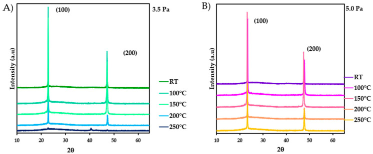
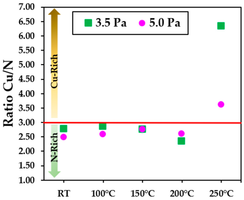
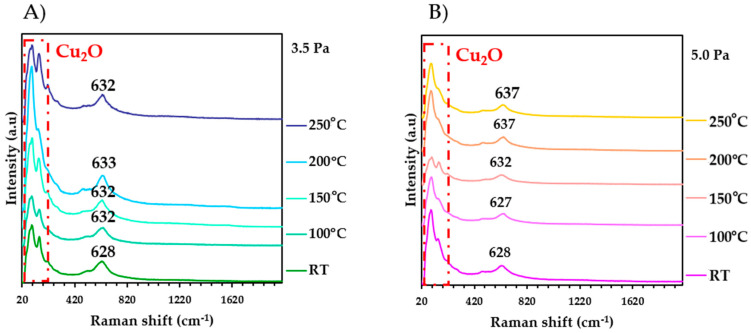
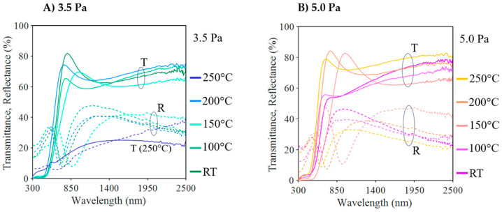
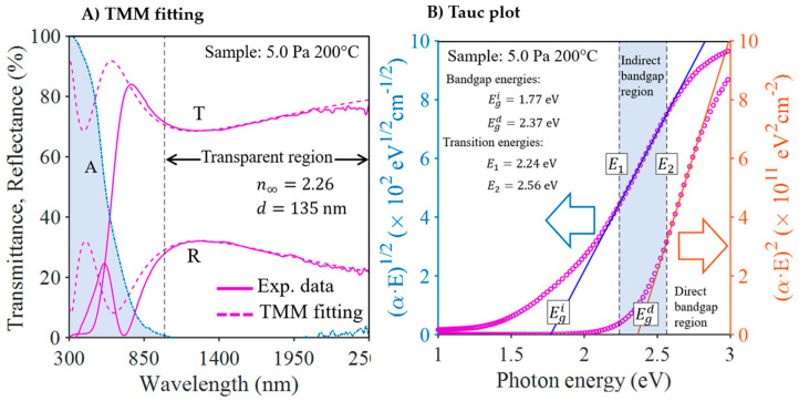
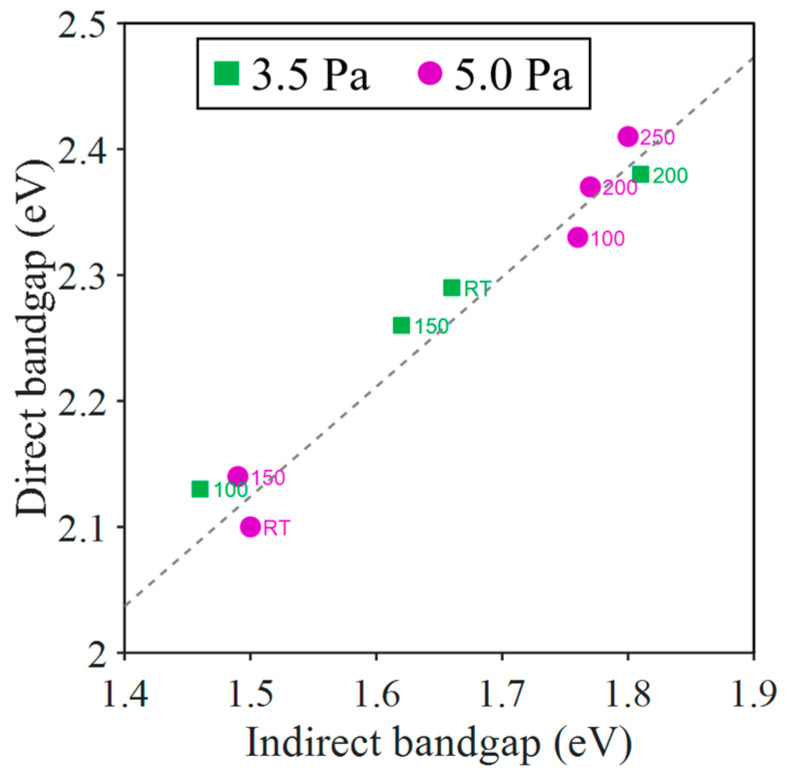
The pursuit of efficient, profitable, and ecofriendly materials has defined solar cell research from its inception to today. Some materials, such as copper nitride (Cu3N), show great promise for promoting sustainable solar technologies. This study employed reactive radio-frequency magnetron sputtering using a pure nitrogen environment to fabricate quality Cu3N thin films to evaluate how both temperature and gas working pressure affect their solar absorption capabilities. Several characterization techniques, including X-ray diffraction (XRD), Rutherford backscattering spectrometry (RBS), Raman spectroscopy, scanning electron microscopy (SEM), nanoindentation, and photothermal deflection spectroscopy (PDS), were used to determine the main properties of the thin films. The results indicated that, at room temperature, it is possible to obtain a material that is close to stoichiometric Cu3N material (Cu/N ratio ≈ 3) with (100) preferred orientation, which was lost as the substrate temperature increases, demonstrating a clear influence of this parameter on the film structure attributed to nitrogen re-emission at higher temperatures. Raman microscopy confirmed the formation of Cu-N bonds within the 628-637 cm-1 range. In addition, the temperature and the working pressure significantly also influence the film hardness and the grain size, affecting the elastic modulus. Finally, the optical properties revealed suitable properties at lower temperatures, including bandgap values, refractive index, and Urbach energy. These findings underscore the potential of Cu3N thin films in solar energy due to their advantageous properties and resilience against defects. This research paves the way for future advancements in efficient and sustainable solar technologies.
Keywords: Cu3N thin films; nanoindentation; optical parameters; reactive magnetron sputtering.
Conflict of interest statement
The authors declare no conflict of interest.
Figures


References
-
- McEvoy A., Castaner L., Markvart T. Solar Cells: Materials, Manufacture and Operation. Academic Press; Cambridge, MA, USA: 2012.
-
- Smith W. Effect of Light on Selenium. Nature. 1873;7:303.
-
- Fritts C.E. On the Fritts selenium cells and batteries. J. Frankl. Inst. 1885;119:221–232. doi: 10.1016/0016-0032(85)90426-0. - DOI
-
- Klassen S. The photoelectric effect: Reconstructing the story for the physics classroom. Sci. Educ. 2011;20:719–731. doi: 10.1007/s11191-009-9214-6. - DOI
-
- Kingsbury E.F., Ohl R.S. Photoelectric properties of ionically bombarded silicon. Bell Syst. Tech. J. 1952;31:802–815. doi: 10.1002/j.1538-7305.1952.tb01407.x. - DOI
Grants and funding
LinkOut - more resources
Full Text Sources
Miscellaneous
