

Printing MEMS: Application of Inkjet Techniques to the Manufacturing of Inertial Accelerometers
- PMID: 38004939
- PMCID: PMC10672808
- DOI: 10.3390/mi14112082
Printing MEMS: Application of Inkjet Techniques to the Manufacturing of Inertial Accelerometers
Abstract
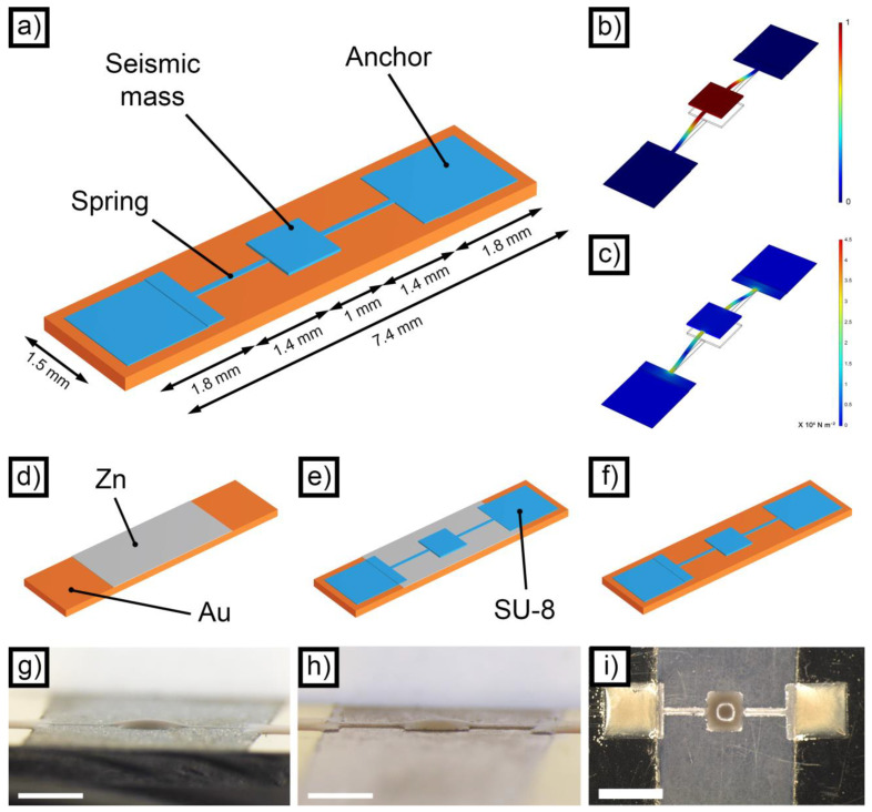
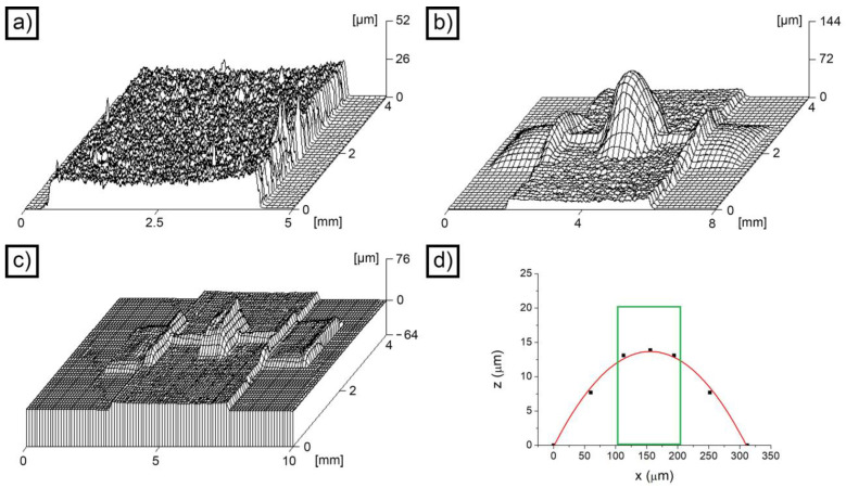
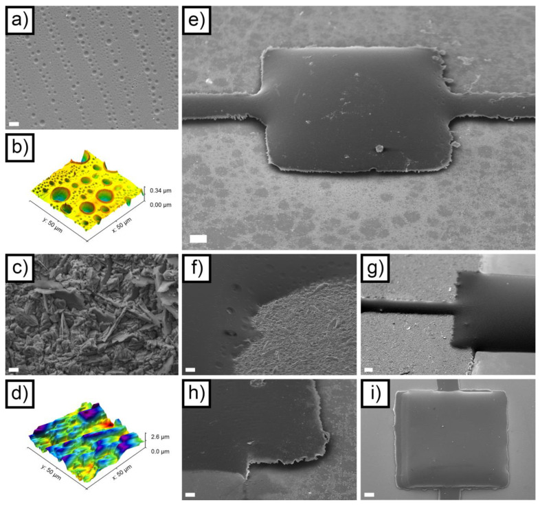
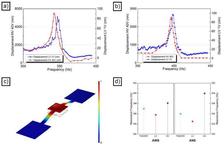
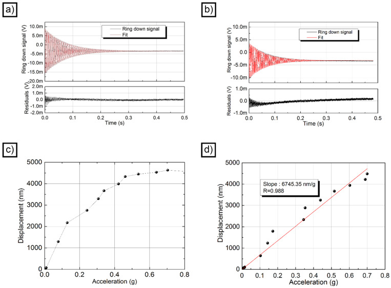
In the last few years, the manufacturing of microelectromechanical systems (MEMS) by means of innovative tridimensional and bidimensional printing technologies has significantly catalyzed the attention of researchers. Inkjet material deposition, in particular, can become a key enabling technology for the production of polymer-based inertial sensors characterized by low cost, high manufacturing scalability and superior sensitivity. In this paper, a fully inkjet-printed polymeric accelerometer is proposed, and its manufacturing steps are described. The manufacturing challenges connected with the inkjet deposition of SU-8 as a structural material are identified and addressed, resulting in the production of a functional spring-mass sensor. A step-crosslinking process allows optimization of the final shape of the device and limits defects typical of inkjet printing. The resulting device is characterized from a morphological point of view, and its functionality is assessed in performing optical readout. The acceleration range of the optimized device is 0-0.7 g, its resolution is 2 × 10⁻³ g and its sensitivity is 6745 nm/g. In general, the work demonstrates the feasibility of polymeric accelerometer production via inkjet printing, and these characteristic parameters demonstrate their potential applicability in a broad range of uses requiring highly accurate acceleration measurements over small displacements.
Keywords: MEMS; SU-8; accelerometer; inkjet printing.
Conflict of interest statement
The authors declare no conflict of interest.
Figures
Similar articles
-
Micro 3D printing of a functional MEMS accelerometer.Microsyst Nanoeng. 2022 Sep 19;8:105. doi: 10.1038/s41378-022-00440-9. eCollection 2022. Microsyst Nanoeng. 2022. PMID: 36133693 Free PMC article.
-
A polymeric piezoelectric MEMS accelerometer with high sensitivity, low noise density, and an innovative manufacturing approach.Microsyst Nanoeng. 2023 Nov 29;9:151. doi: 10.1038/s41378-023-00628-7. eCollection 2023. Microsyst Nanoeng. 2023. PMID: 38033989 Free PMC article.
-
Fully Inkjet Printing Preparation of a Carbon Dots Multichannel Microfluidic Paper-Based Sensor and Its Application in Food Additive Detection.ACS Appl Mater Interfaces. 2021 Dec 8;13(48):57084-57091. doi: 10.1021/acsami.1c14435. Epub 2021 Nov 19. ACS Appl Mater Interfaces. 2021. PMID: 34797049
-
Review of Recent Inkjet-Printed Capacitive Tactile Sensors.Sensors (Basel). 2017 Nov 10;17(11):2593. doi: 10.3390/s17112593. Sensors (Basel). 2017. PMID: 29125584 Free PMC article. Review.
-
An Atlas for the Inkjet Printing of Large-Area Tactile Sensors.Sensors (Basel). 2022 Mar 17;22(6):2332. doi: 10.3390/s22062332. Sensors (Basel). 2022. PMID: 35336503 Free PMC article. Review.
Cited by
-
3D printing of micro-nano devices and their applications.Microsyst Nanoeng. 2025 Feb 27;11(1):35. doi: 10.1038/s41378-024-00812-3. Microsyst Nanoeng. 2025. PMID: 40011446 Free PMC article. Review.
-
RETRACTED: Embedded Sensors with 3D Printing Technology: Review.Sensors (Basel). 2024 Mar 19;24(6):1955. doi: 10.3390/s24061955. Sensors (Basel). 2024. Retraction in: Sensors (Basel). 2024 Dec 13;24(24):7957. doi: 10.3390/s24247957. PMID: 38544218 Free PMC article. Retracted. Review.
References
-
- Adams T.M., Layton R.A. Introductory MEMS: Fabrication and Applications. Springer; Berlin/Heidelberg, Germany: 2010.
-
- Faudzi A.A.M., Sabzehmeidani Y., Suzumori K. Application of Micro-Electro-Mechanical Systems (MEMS) as Sensors: A Review. J. Robot. Mechatron. 2020;32:281–288. doi: 10.20965/jrm.2020.p0281. - DOI
-
- Lyshevski S.E. MEMS and NEMS: Systems, Devices, and Structures. CRC Press; Boca Raton, FL, USA: 2018.
-
- Développement Y. Status of the MEMS Industry 2020–Market and Technology Report. Yole Development; Villeurbanne, France: 2020. Technical Report.
-
- Arh M., Slavič J., Boltežar M. Design principles for a single-process 3d-printed accelerometer—Theory and experiment. Mech. Syst. Signal Process. 2021;152:107475. doi: 10.1016/j.ymssp.2020.107475. - DOI
LinkOut - more resources
Full Text Sources
