Mid-Infrared Mapping of Four-Layer Graphene Polytypes Using Near-Field Microscopy
- PMID: 38007708
- PMCID: PMC10722527
- DOI: 10.1021/acs.nanolett.3c02819
Mid-Infrared Mapping of Four-Layer Graphene Polytypes Using Near-Field Microscopy
Abstract
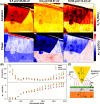
The mid-infrared (MIR) spectral region attracts attention for accurate chemical analysis using photonic devices. Few-layer graphene (FLG) polytypes are promising platforms, due to their broad absorption in this range and gate-tunable optical properties. Among these polytypes, the noncentrosymmetric ABCB/ACAB structure is particularly interesting, due to its intrinsic bandgap (8.8 meV) and internal polarization. In this study, we utilize scattering-scanning near-field microscopy to measure the optical response of all three tetralayer graphene polytypes in the 8.5-11.5 μm range. We employ a finite dipole model to compare these results to the calculated optical conductivity for each polytype obtained from a tight-binding model. Our findings reveal a significant discrepancy in the MIR optical conductivity response of graphene between the different polytypes than what the tight-binding model suggests. This observation implies an increased potential for utilizing the distinct tetralayer polytypes in photonic devices operating within the MIR range for chemical sensing and infrared imaging.
Keywords: Bernal; Few-layer graphene; Mid-IR nano-imaging; Optical conductivity; Raman spectroscopy; Rhombohedral; Scanning near-field optical microscopy; Stacking order.
Conflict of interest statement
The authors declare no competing financial interest.
Figures


Similar articles
-
Experimental Observation of ABCB Stacked Tetralayer Graphene.ACS Nano. 2022 Oct 25;16(10):16617-16623. doi: 10.1021/acsnano.2c06053. Epub 2022 Oct 7. ACS Nano. 2022. PMID: 36205460
-
Electronic structure of few-layer graphene: experimental demonstration of strong dependence on stacking sequence.Phys Rev Lett. 2010 Apr 30;104(17):176404. doi: 10.1103/PhysRevLett.104.176404. Epub 2010 Apr 29. Phys Rev Lett. 2010. PMID: 20482122
-
Stacking Structures of Few-Layer Graphene Revealed by Phase-Sensitive Infrared Nanoscopy.ACS Nano. 2015 Jul 28;9(7):6765-73. doi: 10.1021/acsnano.5b02813. Epub 2015 Jun 15. ACS Nano. 2015. PMID: 26050795
-
Mapping of Bernal and non-Bernal stacking domains in bilayer graphene using infrared nanoscopy.Nanoscale. 2017 Mar 23;9(12):4191-4195. doi: 10.1039/c7nr00713b. Nanoscale. 2017. PMID: 28287222
-
Imaging stacking order in few-layer graphene.Nano Lett. 2011 Jan 12;11(1):164-9. doi: 10.1021/nl1032827. Epub 2010 Dec 1. Nano Lett. 2011. PMID: 21121668
Cited by
-
Metal-Semiconductor Behavior along the Line of Stacking Order Change in Gated Multilayer Graphene.Materials (Basel). 2024 Apr 21;17(8):1915. doi: 10.3390/ma17081915. Materials (Basel). 2024. PMID: 38673272 Free PMC article.
-
Probing Polymorphic Stacking Domains in Mechanically Exfoliated Two-Dimensional Nanosheets Using Atomic Force Microscopy and Ultralow-Frequency Raman Spectroscopy.Nanomaterials (Basel). 2024 Feb 9;14(4):339. doi: 10.3390/nano14040339. Nanomaterials (Basel). 2024. PMID: 38392712 Free PMC article.
References
-
- Du Z.; Zhang S.; Li J.; Gao N.; Tong K. Mid-Infrared Tunable Laser-Based Broadband Fingerprint Absorption Spectroscopy for Trace Gas Sensing: A Review. Appl. Sci. 2019, 9, 338.10.3390/app9020338. - DOI
-
- Fang Y.; Ge Y.; Wang C.; Zhang H. Mid-Infrared Photonics Using 2D Materials: Status and Challenges. Laser Photonics Rev. 2020, 14, 1900098.10.1002/lpor.201900098. - DOI
-
- Singh R.; Su P.; Kimerling L.; Agarwal A.; Anthony B. W. Towards on-chip mid infrared photonic aerosol spectroscopy. Appl. Phys. Lett. 2018, 113, 231107.10.1063/1.5058694. - DOI
-
- Chen H.; Gao L.; Qin Z.; Ge Y.; Khan K.; Song Y.; Xie G.; Xu S.; Zhang H. Recent advances of low-dimensional materials in Mid-and Far-infrared photonics. Appl, Mater. Today 2020, 21, 100800.10.1016/j.apmt.2020.100800. - DOI
LinkOut - more resources
Full Text Sources
Miscellaneous

