

Universal selective transfer printing via micro-vacuum force
- PMID: 38008810
- PMCID: PMC10679119
- DOI: 10.1038/s41467-023-43342-8
Universal selective transfer printing via micro-vacuum force
Erratum in
-
Author Correction: Universal selective transfer printing via micro-vacuum force.Nat Commun. 2023 Dec 6;14(1):8071. doi: 10.1038/s41467-023-44070-9. Nat Commun. 2023. PMID: 38057318 Free PMC article. No abstract available.
Abstract
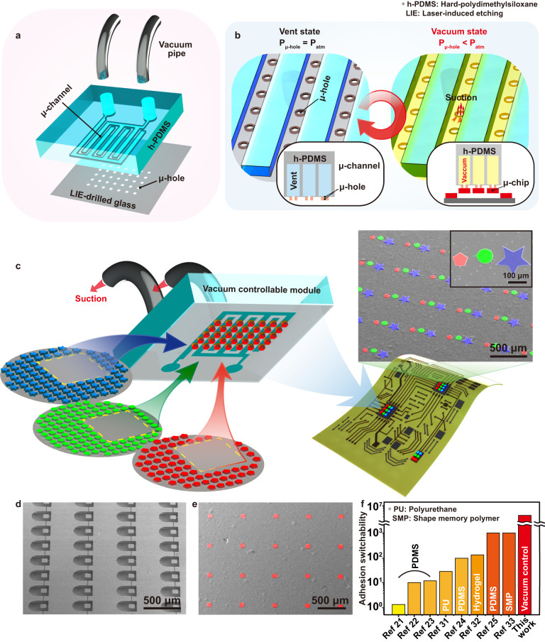
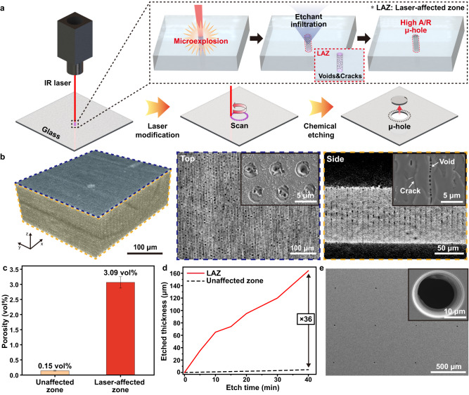
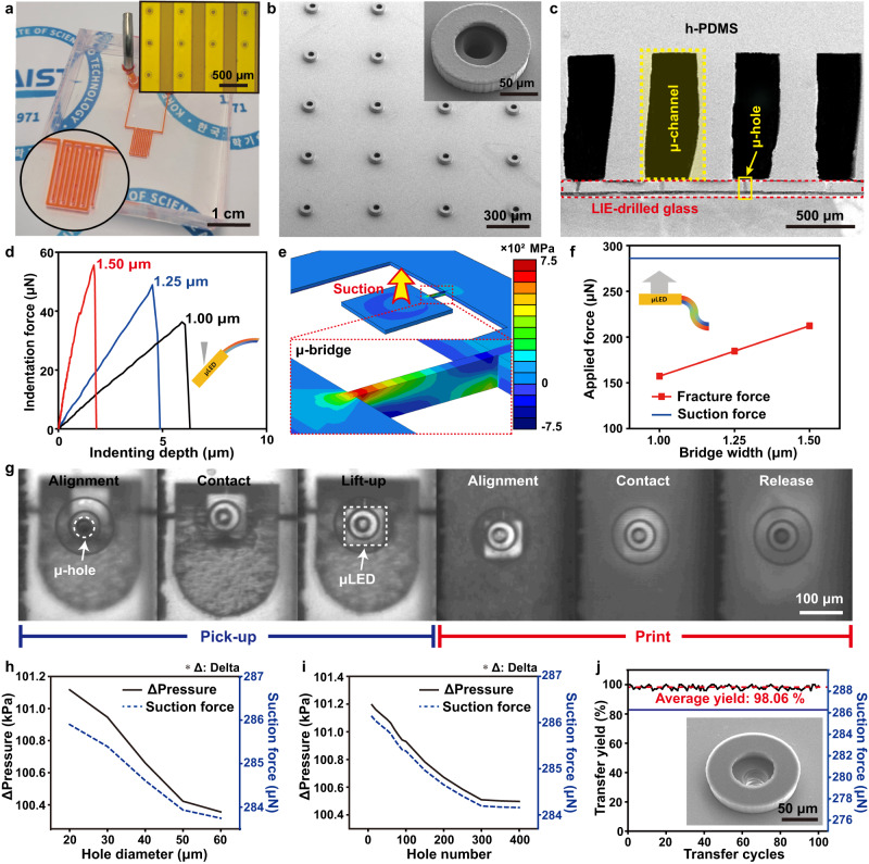
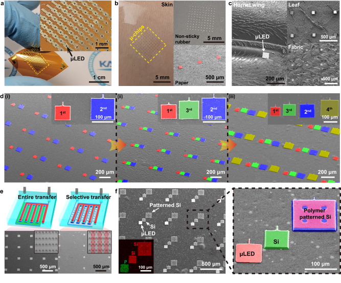
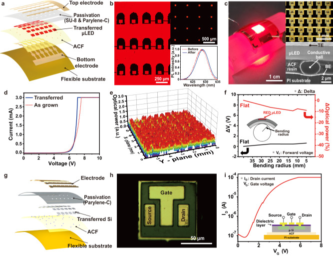
Transfer printing of inorganic thin-film semiconductors has attracted considerable attention to realize high-performance soft electronics on unusual substrates. However, conventional transfer technologies including elastomeric transfer printing, laser-assisted transfer, and electrostatic transfer still have challenging issues such as stamp reusability, additional adhesives, and device damage. Here, a micro-vacuum assisted selective transfer is reported to assemble micro-sized inorganic semiconductors onto unconventional substrates. 20 μm-sized micro-hole arrays are formed via laser-induced etching technology on a glass substrate. The vacuum controllable module, consisting of a laser-drilled glass and hard-polydimethylsiloxane micro-channels, enables selective modulation of micro-vacuum suction force on microchip arrays. Ultrahigh adhesion switchability of 3.364 × 10⁶, accomplished by pressure control during the micro-vacuum transfer procedure, facilitates the pick-up and release of thin-film semiconductors without additional adhesives and chip damage. Heterogeneous integration of III-V materials and silicon is demonstrated by assembling microchips with diverse shapes and sizes from different mother wafers on the same plane. Multiple selective transfers are implemented by independent pressure control of two separate vacuum channels with a high transfer yield of 98.06%. Finally, flexible micro light-emitting diodes and transistors with uniform electrical/optical properties are fabricated via micro-vacuum assisted selective transfer.
© 2023. The Author(s).
Conflict of interest statement
The authors declare no competing interests.
Figures
Similar articles
-
Adhesion performance study of a novel microstructured stamp for micro-transfer printing.Soft Matter. 2021 May 19;17(19):4989-4997. doi: 10.1039/d0sm02161j. Soft Matter. 2021. PMID: 33899836
-
Laser-driven noncontact bubble transfer printing via a hydrogel composite stamp.Proc Natl Acad Sci U S A. 2024 Jan 30;121(5):e2318739121. doi: 10.1073/pnas.2318739121. Epub 2024 Jan 24. Proc Natl Acad Sci U S A. 2024. PMID: 38266054 Free PMC article.
-
Laser-driven programmable non-contact transfer printing of objects onto arbitrary receivers via an active elastomeric microstructured stamp.Natl Sci Rev. 2020 Feb;7(2):296-304. doi: 10.1093/nsr/nwz109. Epub 2019 Aug 6. Natl Sci Rev. 2020. PMID: 34692045 Free PMC article.
-
High-performance printed electronics based on inorganic semiconducting nano to chip scale structures.Nano Converg. 2020 Oct 9;7(1):33. doi: 10.1186/s40580-020-00243-6. Nano Converg. 2020. PMID: 33034776 Free PMC article. Review.
-
Technological Breakthroughs in Chip Fabrication, Transfer, and Color Conversion for High-Performance Micro-LED Displays.Adv Mater. 2023 Oct;35(43):e2204947. doi: 10.1002/adma.202204947. Epub 2023 Feb 15. Adv Mater. 2023. PMID: 35950613 Review.
Cited by
-
Picoliter-Volume Isothermal Titration Calorimetry Using Parylene Chip Calorimeter Integrated with on-Demand Droplet Microfluidics.Small. 2025 Aug;21(32):e2504872. doi: 10.1002/smll.202504872. Epub 2025 Jun 16. Small. 2025. PMID: 40519093 Free PMC article.
-
Shape memory polymer surfaces with controllable roughness for multiscale switchable dry adhesion.Nat Commun. 2025 May 28;16(1):4954. doi: 10.1038/s41467-025-60220-7. Nat Commun. 2025. PMID: 40436828 Free PMC article.
-
Human-Centric, Three Dimensional Micro Light-Emitting Diodes for Cosmetic and Medical Phototherapy.Adv Sci (Weinh). 2025 Mar;12(10):e2416716. doi: 10.1002/advs.202416716. Epub 2025 Feb 17. Adv Sci (Weinh). 2025. PMID: 39960366 Free PMC article.
-
Intrinsically-Stretchable and Patternable Quantum Dot Color Conversion Layers for Stretchable Displays in Robotic Skin and Wearable Electronics.Adv Mater. 2025 Aug;37(32):e2420633. doi: 10.1002/adma.202420633. Epub 2025 May 6. Adv Mater. 2025. PMID: 40326949 Free PMC article.
-
Recent Advances in Tactile Sensory Systems: Mechanisms, Fabrication, and Applications.Nanomaterials (Basel). 2024 Mar 4;14(5):465. doi: 10.3390/nano14050465. Nanomaterials (Basel). 2024. PMID: 38470794 Free PMC article. Review.
References
-
- Behrman K, Kymissis I. Micro light-emitting diodes. Nat. Electron. 2022;5:564–573. doi: 10.1038/s41928-022-00828-5. - DOI
LinkOut - more resources
Full Text Sources
