. 2023 Nov 27:9:149.
doi: 10.1038/s41378-023-00625-w. eCollection 2023.

Vertical serpentine interconnect-enabled stretchable and curved electronics

Affiliations

Vertical serpentine interconnect-enabled stretchable and curved electronics

Rui Jiao et al. Microsyst Nanoeng. .

Abstract

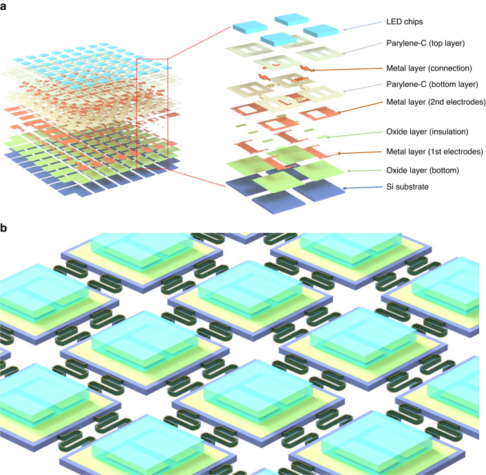
Stretchable and curved electronic devices are a promising technology trend due to their remarkable advantages. Many approaches have been developed to manufacture stretchable and curved electronics. Here, to allow such electronics to better serve practical applications, ranging from wearable devices to soft robotics, we propose a novel vertical serpentine conductor (VSC) with superior electrical stability to interconnect functional devices through a silicon-based microfabrication process. Conformal vacuum transfer printing (CVTP) technology was developed to transfer the networked platform onto complex curved surfaces to demonstrate feasibility. The mechanical and electrical performance were investigated numerically and experimentally. The VSC interconnected network provides a new approach for stretchable and curved electronics with high stretchability and reliability.

Keywords: Electrical and electronic engineering; Structural properties.


Conflict of interest statement

Conflict of interestThe authors declare no competing interests.

Figures

Fig. 1
Fig. 1. Schematic diagram of VSC-enabled curved electronics.
a Curved electronics interconnected with vertical serpentine conductors. b Magnified pictures of curved electronics in (a). c Schematic diagram of the vertical serpentine conductor, including three layers, where the metal layer is arranged near the mechanical neutral plane
Fig. 2
Fig. 2. Design concept of the VSC-enabled stretchable electronic device.
a The structure and material details for the multilayer of an 8 × 8 LED array. b Three-dimensional stretchable and curved display in a planar form
Fig. 3
Fig. 3. Images of the functional device.
a A photograph of an 8 × 8 LED array with released VSCs hung by a tweezer. b SEM image of released VSCs between functional island nodes in (a). c A magnified image of the VSC structure in (b). d A photograph of the 8 × 8 LED array wrapped on a finger. e, f Photographs of the 8 × 8 LED array bent in different directions while maintaining structural integrity and electrical properties
Fig. 4
Fig. 4. Schematic of conformal vacuum transfer printing (CVTP) processes.
a Functional device preparation. b Picking up functional device. c Hemispherical mold preparation. d Printing device onto hemispherical mold. e Complete transfer
Fig. 5
Fig. 5. Images of curved displays.
a Image of the 8 × 8 LED array packaged on a hemispherical mold. b Image of the 8 × 8 LED array packaged on a saddle-shaped substrate. c Image of the 8 × 8 LED array wrapped on an irregular curved substrate. d A partially magnified image of the LED array interconnected with VSCs in (a). e A partially magnified image in (b). f A partially magnified image in (c). g Image of all LEDs lit up on the curved substrate. hl Images of the curved display presenting the letters “HKUST” individually
Fig. 6
Fig. 6. FEA results for 8 × 8 island nodes interconnected with VSCs covered intimately onto curved surfaces.
a An overall view of the stress distribution for the curved device covering the hemispherical surface. b A magnified picture of the stress distribution in the middle region in (a). c An overall view of the stress distribution for the curved device covered on the saddle surface. d A magnified picture of the stress distribution in the marginal region in (c)
Fig. 7
Fig. 7. Silicon-based microfabrication process for stretchable and curved electronics.
a, b Pattern on the reverse side of the silicon wafer. ce Two metal layer deposition and patterning for electrodes on islands. f Groove patterning and etching using the DRIE system. gj Materials deposition to fill in the groove and pattern the Parylene-C layers and metal layer to form a sandwich structure for interconnects between islands. k Patterning and etching the top layer of Parylene-C. l Dry etch the silicon substrate from the reverse side using DRIE and RIE systems to release the conductors and obtain a free standing system

References

    1. Kim DH, et al. Stretchable, curvilinear electronics based on inorganic materials. Adv. Mater. 2010;22:2108–2124. doi: 10.1002/adma.200902927. - DOI - PubMed
    1. Gao W, et al. Fully integrated wearable sensor arrays for multiplexed in situ perspiration analysis. Nature. 2016;529:509. doi: 10.1038/nature16521. - DOI - PMC - PubMed
    1. Shi Q, et al. Progress in wearable electronics/photonics—moving toward the era of artificial intelligence and internet of things. InfoMat. 2020;2:1131–1162. doi: 10.1002/inf2.12122. - DOI
    1. Ko HC, et al. A hemispherical electronic eye camera based on compressible silicon optoelectronics. Nature. 2008;454:748. doi: 10.1038/nature07113. - DOI - PubMed
    1. Song YM, et al. Digital cameras with designs inspired by the arthropod eye. Nature. 2013;497:95. doi: 10.1038/nature12083. - DOI - PubMed