

A Perovskite-Graphene Device for X-ray Detection
- PMID: 38046671
- PMCID: PMC10688579
- DOI: 10.1016/j.carbon.2023.118586
A Perovskite-Graphene Device for X-ray Detection
Abstract
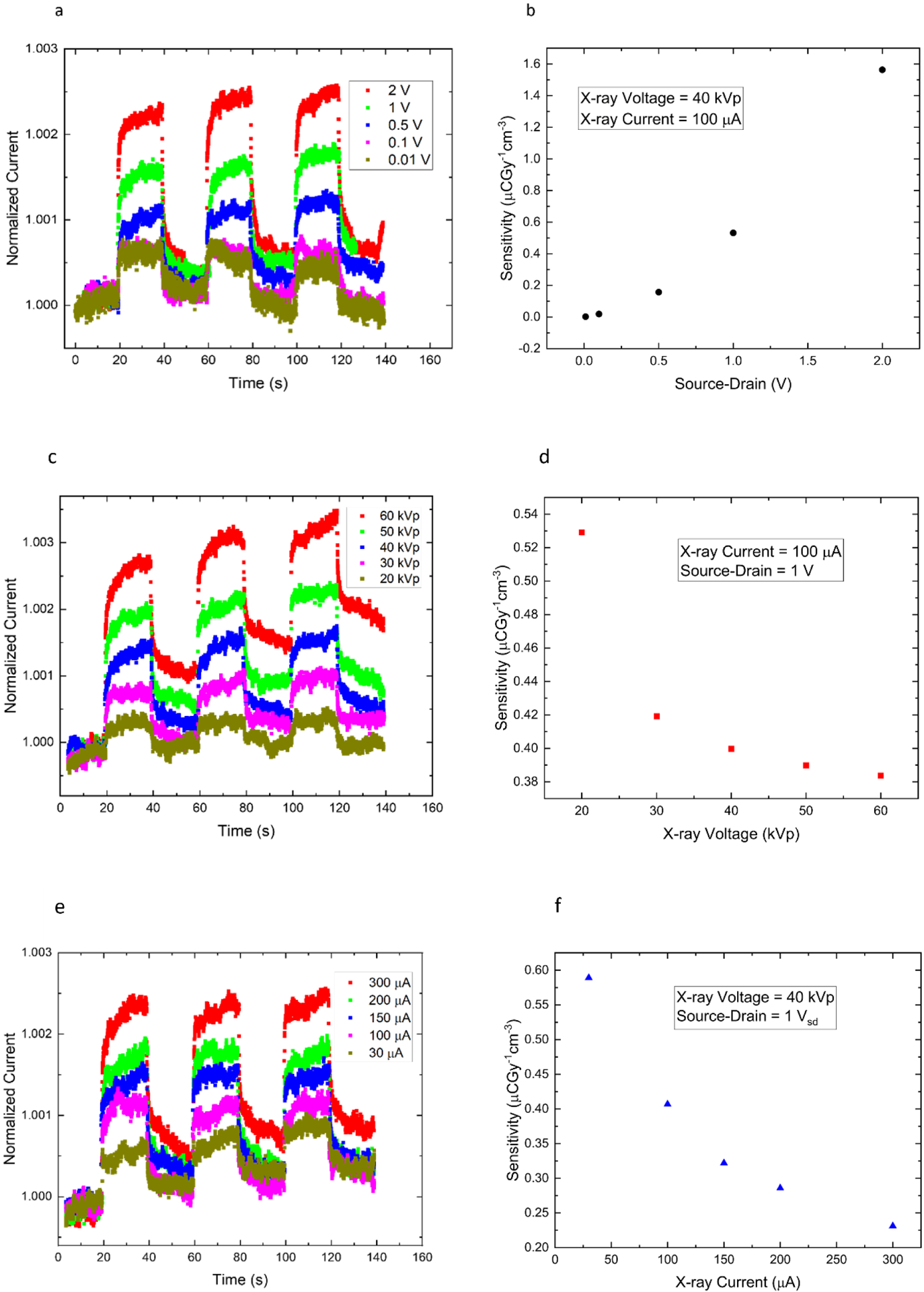
This study examines a perovskite-based graphene field effect transistor (P-GFET) device for X-ray detection. The device architecture consisted of a commercially available GFET-S20 chip, produced by Graphenea, with a layer of methylammonium lead iodide (MAPbI3) perovskite spin coated onto the top of it. This device was exposed to the field of a molybdenum target X-ray tube with beam settings between 20-60 kVp (X-ray tube voltage) and 30-300 uA (X-ray tube current). Dose measurements were taken with an ion-chamber and thermo-luminescent dosimeters and used to determine the sensitivity of the device as a function of the X-ray tube voltage and current, as well as source-drain voltage. The X-ray tube was also simulated in this work with GEANT4 and MCNP to determine the dose rate and power incident on the device during irradiation. These simulations were then used to determine the responsivity as a function of the X-ray tube voltage and current, as well as the source-drain voltage. Overall, a strong positive correlation between sensitivity and source-drain voltage was found. Conversely, the sensitivity was found to decrease - roughly exponentially - as a function of both the X-ray tube current and energy. Similar trends were seen with responsivity. We report the models used for the study as well as address the feasibility of the device as a low-energy (< 70 keV) X-ray photon detector.
Keywords: GFET; Graphene; X-ray; perovskite; radiation detection.
Conflict of interest statement
Declaration of interests The authors declare that they have no known competing financial interests or personal relationships that could have appeared to influence the work reported in this paper.
Figures


References
-
- He Y, Petryk M, Liu Z, Chica DG, Hadar I, Leak C, Ke W, Spanopoulos I, Lin W, Chung DY, Wessels BW, He Z, and Kanatzidis MG, “CsPbBr3 perovskite detectors with 1.4% energy resolution for high-energy γ-rays,” Nat Photonics 15(1), 36–42 (2021).
-
- Kang J, and Cho JH, “Organic-inorganic hybrid perovskite electronics,” Physical Chemistry Chemical Physics 22(24), 13347–13357 (2020). - PubMed
-
- Zhou Z, Qiang Z, Sakamaki T, Takei I, Shang R, and Nakamura E, “Organic/Inorganic Hybrid p-Type Semiconductor Doping Affords Hole Transporting Layer Free Thin-Film Perovskite Solar Cells with High Stability,” ACS Appl Mater Interfaces, (2019). - PubMed
-
- Li S, Zhang C, Song JJ, Xie X, Meng JQ, and Xu S, “Metal halide perovskite single crystals: From growth process to application,” Crystals (Basel) 8(5), (2018).
Grants and funding
LinkOut - more resources
Full Text Sources