Review
. 2023 Dec 7;16(1):45.
doi: 10.1007/s40820-023-01254-8.

Recent Advances in Patterning Strategies for Full-Color Perovskite Light-Emitting Diodes

Affiliations
Review

Recent Advances in Patterning Strategies for Full-Color Perovskite Light-Emitting Diodes

Gwang Heon Lee et al. Nanomicro Lett. .

Abstract

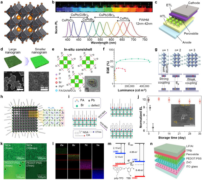
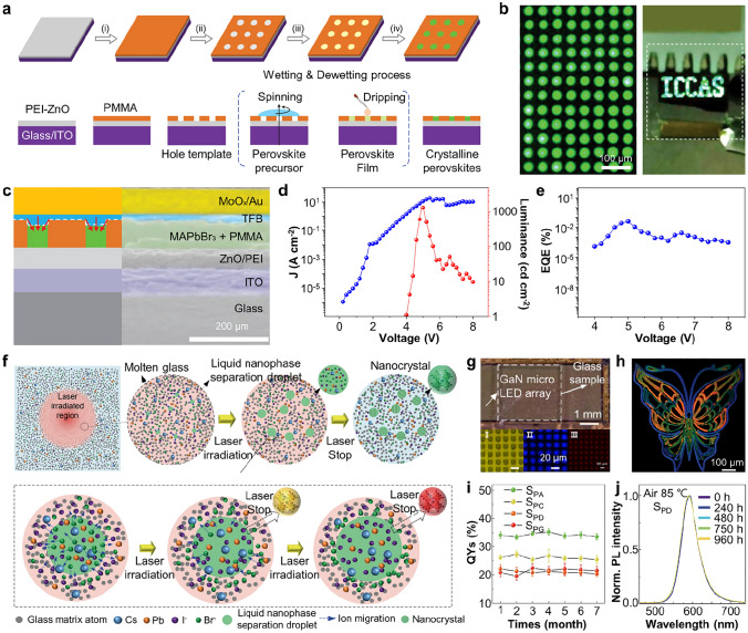
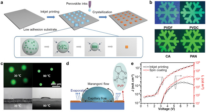
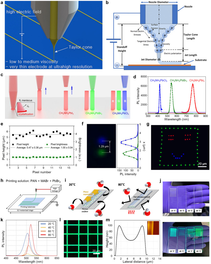
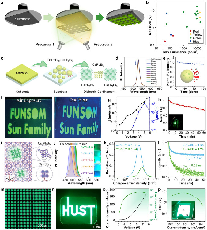
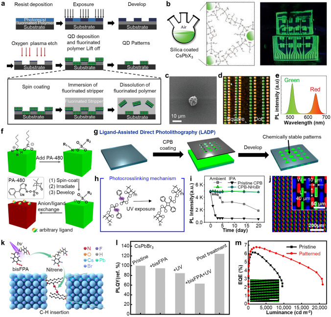
Metal halide perovskites have emerged as promising light-emitting materials for next-generation displays owing to their remarkable material characteristics including broad color tunability, pure color emission with remarkably narrow bandwidths, high quantum yield, and solution processability. Despite recent advances have pushed the luminance efficiency of monochromic perovskite light-emitting diodes (PeLEDs) to their theoretical limits, their current fabrication using the spin-coating process poses limitations for fabrication of full-color displays. To integrate PeLEDs into full-color display panels, it is crucial to pattern red-green-blue (RGB) perovskite pixels, while mitigating issues such as cross-contamination and reductions in luminous efficiency. Herein, we present state-of-the-art patterning technologies for the development of full-color PeLEDs. First, we highlight recent advances in the development of efficient PeLEDs. Second, we discuss various patterning techniques of MPHs (i.e., photolithography, inkjet printing, electron beam lithography and laser-assisted lithography, electrohydrodynamic jet printing, thermal evaporation, and transfer printing) for fabrication of RGB pixelated displays. These patterning techniques can be classified into two distinct approaches: in situ crystallization patterning using perovskite precursors and patterning of colloidal perovskite nanocrystals. This review highlights advancements and limitations in patterning techniques for PeLEDs, paving the way for integrating PeLEDs into full-color panels.

Keywords: Electroluminescence; Full-color display; High-resolution patterning; Light-emitting diode; Perovskite.


Conflict of interest statement

The authors declare no interest conflict. They have no known competing financial interests or personal relationships that could have appeared to influence the work reported in this paper.

Figures

Fig. 1
Fig. 1
The schematic and radar plot of representative MHP patterning techniques. The radar plot illustrates the evaluation of different MHP patterning techniques based on five key factors: uniformity, resolution, throughput, eco-friendness, and multi-color. The uniformity factor indicates the consistency in morphology, shape, and thickness of each patterned pixels. The eco-friendness factor assesses the energy consumption per unit patterned pixel and the potential generation of chemical contaminants during the patterning process
Fig. 2
Fig. 2
Strategy for highly efficient PeLEDs. a Schematic of 3D cubic MHP crystal structure of ABX3. Reproduced with permission [47]. Copyright 2019 American Chemical Society. b Representative perovskite colloidal solution and photoluminescence (PL) spectra of MHP. Reproduced with permission [48]. Copyright 2015 American Chemical Society. c) Schematic of PeLED device structure. d Schematics (top) and corresponding scanning electron microscope (SEM) images before (bottom left) and after (bottom right) the nanocrystal pinning process. Reproduced with permission [60]. Copyright 2015 American Association for the Advancement of Science (AAAS). e Schematic of in-situ core/shell perovskite with BPA treatment. The inset shows transmission electron microscope (TEM) image of in-situ core/shell perovskite. f EQE versus luminance of in-situ core/shell PeLED. Reproduced with permission [14]. Copyright 2022 Springer Nature. g Schematic crystal structures of quasi-2D perovskites with varying n values and their corresponding electronic properties influenced by quantum- and dielectric-confinement effects. Reproduced with permission [61]. Copyright 2021 Springer Nature. h Schematic of GA doped FAPbBr3 PeNCs. Reproduced with permission [69]. Copyright 2021 Springer Nature. i Schematic illustration of ligand exchange process of PeNCs with NSA. Reproduced with permission [73]. Copyright 2021 American Chemical Society. j Time-related storage stability of normal CsPbI3 and Pb capped CsPbI3-0.1 PeLEDs under ambient environment. The inset shows TEM image of CsPbI3 with 0.3-nm-thick Pb shell. Reproduced with permission [81]. Copyright 2018 American Chemical Society. k EL images of quasi-2D PeLEDs with NiOx (top) and PEDOT:PSS (bottom) as HTL at various operation time. Reproduced with permission [87]. Copyright 2018, Wiley–VCH. l EDS elemental mapping image of ZnO/CsPbBr3/NiO/ITO structure. Reproduced with permission [89]. Copyright 2018 American Chemical Society. m Schematic representation of p-type doping mechanism involving electron transfer from Poly-TPD to TBB. The inset shows chemical structure of each molecule. Reproduced with permission [89]. Copyright 2020 Elsevier. n Schematic illustration of PeLED device structure with moth-eye nanostructured layer. Reproduced with permission [95]. Copyright 2019, Wiley–VCH
Fig. 3
Fig. 3
a Schematic illustration depicting the top-down photolithography strategy using perovskite precursors and negative photoresist. b Schematic representation of the direct in-situ photolithography process utilizing photosensitive PPR. c Multi-color (red and green) patterns of squares with the width of 250 μm. d Single-color cartoon image. e Cross section SEM image showing perovskite stripe patterns polymerized with the same UV exposure time. f Radial PL intensity distribution of a circle pixel. Reproduced with permission [19]. Copyright 2022, Springer Nature. g Schematic illustration showing the peel-off fabrication process with a parylene-C layer positioned between the photoresist and perovskite layer. h Multi-color (red and green) perovskite patterns of circles with a diameter of 50 μm and i single-color cartoon image of a panda. j J–V–L curve and k EQE and current efficiency curve measured from PeLEDs using the patterned perovskite layer. Reproduced with permission [20]. Copyright 2020, American Chemical Society
Fig. 4
Fig. 4
a Schematic illustration showing the patterning process utilizing the hole template fabricated through E-beam lithography. b EL image of green perovskite circle patterns and “ICCAS” logo photography showing perovskite micro-LED arrays. c Schematic illustrating the device structure and cross section SEM image of PeLEDs. d JVL and e EQE curve of the fabricated PeLEDs employing perovskite layers. Reproduced with permission [36]. Copyright 2020, Wiley–VCH. f Schematic of the formation of CsPb(Cl1-xBrx)3 nanocrystals induced by ultrafast laser irradiation. g Optical microscope image showing the structure of micro-PeLED devices. h Multi-color patterned image obtained using ultrafast laser-assisted lithography. i Changes in PLQYs of CsPb(Cl1-xBrx)3 nanocrystals exposed to ethanol and j PL spectra after heating at 85 °C for 960 h. Reproduced with permission [34]. Copyright 2022, The American Association for the Advancement of Science (AAAS)
Fig. 5
Fig. 5
a Schematic illustration of the inkjet printing technique using in-situ crystallization of the perovskite precursor. Reproduced with permission [147]. Copyright 2016, Wiley–VCH. b PL images of PeNC patterns printed on various polymer substrates. c Fluorescence images (top) and cross-sectional contact angle images (bottom) of inkjet-printed dot patterns with different substrate temperatures of 30 and 90 ℃. Reproduced with permission [150]. Copyright 2019, Wiley–VCH. d Schematic diagram of the formation principle of coffee ring effect with PVP layer. e J–V–L curves of PeLEDs fabricated by spin-coating and inkjet printing. Reproduced with permission [40]. Copyright 2021, Wiley–VCH
Fig. 6
Fig. 6
a Schematic diagram illustrating operational modes for stable performance in drop-on-demand inkjet printing. Reproduced with permission [155]. Copyright 2011, American Institute of Physics. b Schematic showing crystallization of PeNCs with different speed of nucleation (top) and crystallization process of PVP containing precursor ink (bottom). c PL images (top) and thickness profile (bottom) of crystallized single dot pattern in ambient condition (left), vacuum condition with substrate temperature of 20 ℃ (middle) and 30 ℃ (right). Reproduced with permission [96]. Copyright 2019, American Chemical Society. d Film thickness profile of crystallized single dot pattern (top) and SEM images (bottom) dried at different vacuum level. The insets show 3D morphology of inkjet-printed pattern. Scale bar is 100 nm. e EL image of white PeLED at 5 V. The inset shows RGB pixelated patterns. Scale bar is 100 μm. f J–V–L curves of printed RGB PeLEDs. Reproduced with permission [22]. Copyright 2021, American Chemical Society. g Schematic device structure of all-inkjet-printed PeLED. h Optical microscope images of composite film printed at different temperature. i L–V curves of all-inkjet-printed flexible PeLEDs according to bending cycles. Reproduced with permission [23]. Copyright 2021, Wiley–VCH. j Schematic illustration of the inkjet printing process for fabrication of single-crystal perovskite-embedded PDMS. k Optical images of single-crystal growth according to the growth time. l The size of single crystals depending on the ink concentration. m Fluorescence images of complicated single-crystal perovskite patterns embedded in PDMS films. Reproduced with permission [159]. Copyright 2020, American Chemical Society
Fig. 7
Fig. 7
a Schematic illustration depicting the operational principle of E-jet printing. Reproduced with permission [26]. Copyright 2015, Springer Nature. b Schematic illustration showing the formation Taylor cone by applied voltage. Reproduced with permission [27]. Copyright 2021, Springer Nature. c Schematic illustration describing the formation process of 3D perovskite nanopixels through meniscus-guided crystallization. d PL spectra of red, green and blue 3D perovskite nanopixels. e The height and brightness distribution of 3D nanopixels. f High-resolution pixelated image with a gap of 1.29 μm and intensity profiling of multi-color pixels. g PL image of nanopixel patterns with RGB multi-color perovskite, showing a “Smile face”. Reproduced with permission [28]. Copyright 2021, American Chemical Society. h Schematic of the E-jet printing system with high viscosity printing solution. i The vapor-induced phase separation effect according to the processing temperature. j Photograph and k PL intensity of E-jet printed perovskite patterns according to the processing temperature. l PL image of single-color line patterns. Scale bar is 20 μm. m AFM image and line profile of the pattern. Reproduced with permission [29]. Copyright 2022, American Chemical Society
Fig. 8
Fig. 8
a Schematic illustration describing the co-evaporation process. b Max luminance and EQE chart for PeLEDs fabricated by the thermal evaporation of perovskite layers. c Schematic illustration showing the formation of matrix structure with CsPbBr3 embedded in CsPb2Br5. d Time-dependent PL spectra and e the PL peak intensity of perovskite films under air exposure (~ 60% humidity). f PL images of patterned perovskite films captured immediately after exposure to air conditions (left) and after one year in the ambient atmosphere (right). g J–V–L curve and h time-dependent EQE curve of PeLEDs employing the CsPbBr3/Cs4PbBr6 films. Reproduced with permission [32]. Copyright 2019, Wiley–VCH. i Schematic illustration showing the matrix structure with CsPbBr3 embedded in Cs4PbBr6. j PL intensity of perovskite films with various Cs/Pb ratios. k The simulated radiative efficiency versus charge carrier density and l time-resolved photoluminescence (TRPL) of perovskite films with Cs/Pb ratio of 1.56 and 1.24. m Fluorescence microscope image of the patterned perovskite film and n EL image of PeLEDs. o J–V–L curve and p EQE versus current density curve of large-area PeLEDs. Reproduced with permission [43]. Copyright 2021, Springer Nature
Fig. 9
Fig. 9
a Schematic illustration showing orthogonal photolithography process with fluorinated layer. Reproduced with permission [119]. Copyright 2018, Wiley–VCH. b Gel-type silica-coated perovskite precursor (left) and PL image of printed film on flexible PET substrate (right). c SEM image of silica-coated perovskite dot pattern with radius of 5 μm. d Periodic red/green square (left) and dot (right) patterns of silica-coated perovskites. e PL intensity of red and green patterns. Reproduced with permission [188]. Copyright 2020, Wiley–VCH. f Schematic illustration showing direct photolithography with photosensitive oxime sulfonate ester. Reproduced with permission [190]. Copyright 2021, American Chemical Society. g Schematic of ligand-assisted direct photolithography patterning. h Schematic illustration showing photocrosslinking mechanism using the cinnamoyl group on the ligand under UV exposure. i PL intensity versus time graph of pristine CPB and CPB-NH3Br under ambient, and IPA conditions. j PL image of RGB pixelated perovskite patterns by LADP patterning method. Reproduced with permission [191]. Copyright 2021, American Chemical Society. k Schematic of ligand crosslinking by bisazide under UV exposure. l Relative PLQY of CsPbBr3 films under different treatments in direct optical patterning processes with ligand crosslinker. m EQE performances of EL devices of pristine and patterned by DOPPLCER. The inset shows patterned EL device. Scale bar is 200 μm. Reproduced with permission [21]. Copyright 2022, The American Association for the Advancement of Science (AAAS)
Fig. 10
Fig. 10
a PL image of sequential inkjet-printed RGB PeNC patterns through halide exchange using tert-butyl chloride and tert-butyl iodide. Reproduced with permission [196]. Copyright 2019, Wiley–VCH. b Illustration of pristine and UV-crosslinked PeNC degradation mechanisms under UV and ambient environment. c Time-dependent changes in relative PL intensity of pristine PeNCs, PeNCs with PI, and PeNCs with LS under UV exposure. d J–V–L curves of PeLEDs fabricated by inkjet printing of PeNCs. The inset shows inkjet-printed red and green EL device. Reproduced with permission [24]. Copyright 2021, Wiley–VCH. e Schematic illustration of droplet rheology with ternary solvent ink system. f Topographical profiles of inkjet-printed PeNC thin films obtained using a binary and ternary solvent ink system. g J–V–L curves and h EQE versus current density curves of inkjet-printed PeLEDs using the binary and ternary solvent ink system. Reproduced with permission [41]. Copyright 2022, Wiley–VCH. i Schematic of PeLED structure patterned by inkjet printing. j Fluorescence images of inkjet-printed PeNC arrays on PVK (top) and SDS (bottom). k J–V–L curves and l EQE–V curves of inkjet-printed RGB PeLEDs. Reproduced with permission [25]. Copyright 2022, Wiley–VCH
Fig. 11
Fig. 11
a Schematic illustration showing transfer printing process. b Diagram of adhesion versus stimulus considering the two interfaces in stamp/ink/substrate system. Reproduced with permission [204]. Copyright 2018, Springer Nature. c Schematic of mass transfer printing method. d J–V–L curves of red PeLEDs fabricated by transfer printing and spin-coating. e EQE curve of white PeLED. The inset show photograph of white PeLED. Reproduced with permission [30]. Copyright 2022, Wiley–VCH. f Schematic of PeNCs/ETL double layer release process (left) and work of adhesion graph between PDMS stamp and PeNC and PeNC/TPBi double layer (right). g Fluorescence microscopic images displaying pixelated RGB PeNC patterns with a resolution of 2,550 PPI. h J–V–L curves, i EQE versus current density curves, and j Electrochemical impedance analysis results of PeLEDs fabricated by spin-coating, transfer printing, transfer printing without solvent treatment of PeNCs. k Optical microscope images illustrating the EL emisstion from green PeLEDs using high-resolution transfer printing. The inset shows the photograph of green PeLED patterned by transfer printing. l Photograph of skin-attachable ultrathin multi-color PeLED. The inset shows a cross-sectional TEM image of a transfer printed PeLED with a total thickness of ~ 2.6 μm. Reproduced with permission [31]. Copyright 2022, American Association for the Advancement of Science (AAAS)

References

    1. G. Wang, A. Badal, X. Jia, J.S. Maltz, K. Mueller et al., Development of metaverse for intelligent healthcare. Nat. Mach. Intell. 4(11), 922–929 (2022). 10.1038/s42256-022-00549-6 - PMC - PubMed
    1. F.Y. Wang, R. Qin, X. Wang, B. Hu, Metasocieties in metaverse: Metaeconomics and metamanagement for metaenterprises and metacities. IEEE Trans. Comput. Soc. Syst. 9(1), 2–7 (2022). 10.1109/TCSS.2022.3145165
    1. J. Yang, M.K. Choi, U.J. Yang, S.Y. Kim, Y.S. Kim et al., Toward full-color electroluminescent quantum dot displays. Nano Lett. 21(1), 26–33 (2021). 10.1021/acs.nanolett.0c03939 - PubMed
    1. J. Yang, J. Yoo, W.S. Yu, M.K. Choi, Polymer-assisted high-resolution printing techniques for colloidal quantum dots. Macromol. Res. 29(6), 391–401 (2021). 10.1007/s13233-021-9055-y
    1. S.J. Anderson, K.T. Mullen, R.F. Hess, Human peripheral spatial resolution for achromatic and chromatic stimuli: Limits imposed by optical and retinal factors. J. Physiol. 442(1), 47–64 (1991). 10.1113/jphysiol.1991.sp018781 - PMC - PubMed

LinkOut - more resources