. 2024 Feb;11(6):e2307600.
doi: 10.1002/advs.202307600. Epub 2023 Dec 10.

Revealing Two Distinct Formation Pathways of 2D Wurtzite-CdSe Nanocrystals Using In Situ X-Ray Scattering

Affiliations

Revealing Two Distinct Formation Pathways of 2D Wurtzite-CdSe Nanocrystals Using In Situ X-Ray Scattering

Hyo Cheol Lee et al. Adv Sci (Weinh). 2024 Feb.

Abstract

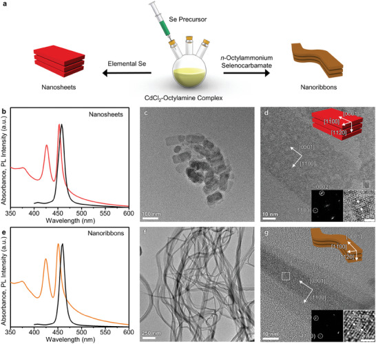
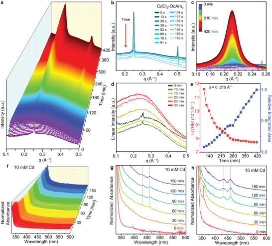
Understanding the mechanism underlying the formation of quantum-sized semiconductor nanocrystals is crucial for controlling their synthesis for a wide array of applications. However, most studies of 2D CdSe nanocrystals have relied predominantly on ex situ analyses, obscuring key intermediate stages and raising fundamental questions regarding their lateral shapes. Herein, the formation pathways of two distinct quantum-sized 2D wurtzite-CdSe nanocrystals - nanoribbons and nanosheets - by employing a comprehensive approach, combining in situ small-angle X-ray scattering techniques with various ex situ characterization methods is studied. Although both nanostructures share the same thickness of ≈1.4 nm, they display contrasting lateral dimensions. The findings reveal the pivotal role of Se precursor reactivity in determining two distinct synthesis pathways. Specifically, highly reactive precursors promote the formation of the nanocluster-lamellar assemblies, leading to the synthesis of 2D nanoribbons with elongated shapes. In contrast, mild precursors produce nanosheets from a tiny seed of 2D nuclei, and the lateral growth is regulated by chloride ions, rather than relying on nanocluster-lamellar assemblies or Cd(halide)2 -alkylamine templates, resulting in 2D nanocrystals with relatively shorter lengths. These findings significantly advance the understanding of the growth mechanism governing quantum-sized 2D semiconductor nanocrystals and offer valuable guidelines for their rational synthesis.

Keywords: 2D nanocrystals; formation mechanism; in situ small-angle X-ray scattering; nanoribbons; nanosheets; quantum-sized semiconductor nanocrystals.


Conflict of interest statement

The authors declare no conflict of interest.

Figures

Figure 1
Figure 1
Synthesis and characterization of 2D CdSe nanosheets and nanoribbons. a) Schematic illustration showing synthesis of 2D CdSe nanosheets (left) and 2D CdSe nanoribbons (right). b) Absorption (red) and PL (black) spectra and c,d) TEM images of 2D CdSe nanosheets. e) Absorption (orange) and PL (black) spectra and f,g) TEM images of 2D CdSe nanoribbons. The upper‐right insets in panels (d) and (g) show the nanocrystal structures and crystal orientation. The lower‐right insets in panels (d) and (g) show magnified TEM images of the white‐dotted rectangular areas, showing the lattice spacings and the corresponding FFT patterns.
Figure 2
Figure 2
Formation of CdSe nanoribbons. a) In situ SAXS patterns depicting the evolution of CdSe nanoribbons, b) the first half of the reaction (0–4 h), and c) the latter half of the reaction (4–8 h). Relative integrated area and linewidth (half‐width at half‐maximum, HWHM) for the first‐order peaks of d) the cluster assemblies (q = 0.237 Å−1) and e) the nanoribbon assemblies (q = 0.210 Å−1) as a function of reaction time. A maximum area value during the observation is set as 1. The scattering intensity of all panels is plotted using a logarithmic scale except for panel (d) and (e) (linear scale). f) Temporal evolution of absorption spectra of a series of aliquots during nanoribbon synthesis. After 1 h of reaction at room temperature (25 °C), the reaction temperature was increased to 70 °C. The position of band‐edge transitions of magic‐sized (CdSe)34 and (CdSe)13 clusters are depicted by a gray star and gray dotted line, respectively. g,h) TEM images of (CdSe)13 cluster assemblies. The ordered region with a striped pattern represents the lamellar structure. Inset in panel (g) shows the magnified image.
Figure 3
Figure 3
Formation of CdSe nanosheets. a) In‐situ SAXS patterns depicting the evolution of CdSe nanosheets. b) Initial 15 frames (corresponding to 0–3 min) of the SAXS patterns magnified near the regime corresponding to the first and second‐order reflections of the lamellar assemblies of CdCl2–OcAm x complexes. c) Magnified SAXS patterns on the regime corresponding to the first‐order reflections of the lamellar assemblies of nanosheets. d) Representative SAXS curves for the initial 30 min. e) Relative integrated area and linewidth for the first‐order peak of the nanosheet assemblies (q = 0.210 Å−1) as a function of reaction time. A maximum area value during the observation is set as 1. The scattering intensity of all panels is plotted using a logarithmic scale except for panel (d) and (e) (linear scale). f) In situ absorption spectra depicting the evolution of CdSe nanosheets at the Cd concentration of 10 mm. g) Selected absorption spectra acquired from panel (f). The gray dashed lines indicate the heavy hole‐ and light hole‐excitonic transitions of nanosheets. h) In situ absorption analysis at the higher Cd concentration (15 mm).
Figure 4
Figure 4
Effect of Cl ions on nanosheet synthesis. a) Absorption spectra and TEM images of CdSe nanosheets synthesized with b) 2.0, c) 3.0, d) 5.0, and e) 10.0 equivalent Cl ions. The absorption spectrum of the controlled sample (1.0 equivalent Cl ions) is presented in panel a for comparison.
Figure 5
Figure 5
Schematic of the two proposed critical pathways for the synthesis of quantum‐sized 2D CdSe nanocrystals: a) nanoribbons and b) nanosheets. The atoms with orange and blue colors represent Cd and Se atoms, respectively. Please note that the illustrations should be interpreted as conceptual representations of growth pathways for 2D nanocrystals, rather than precise depictions of specific structural details (e.g., the structure of nanoclusters and interdigitation between particles).

References

    1. Lee J., Yang J., Kwon S. G., Hyeon T., Nat. Rev. Mater. 2016, 1, 16034.
    1. Fan Z., Zhang H., Chem. Soc. Rev. 2016, 45, 63. - PubMed
    1. Ha S.‐T., Su R., Xing J., Zhang Q., Xiong Q., Chem. Sci. 2017, 8, 2522. - PMC - PubMed
    1. Siefe C., Mehlenbacher R. D., Peng C. S., Zhang Y., Fischer S., Lay A., Mclellan C. A., Alivisatos A. P., Chu S., Dionne J. A., J. Am. Chem. Soc. 2019, 141, 16997. - PMC - PubMed
    1. Park J., An K., Hwang Y., Park J.‐G., Noh H.‐J., Kim J.‐Y., Park J.‐H., Hwang N.‐M., Hyeon T., Nat. Mater. 2004, 3, 891. - PubMed

LinkOut - more resources