

Van Der Waals Semiconductor Based Omnidirectional Bifacial Transparent Photovoltaic for Visual-Speech Photocommunication
- PMID: 38083978
- PMCID: PMC10870018
- DOI: 10.1002/advs.202306408
Van Der Waals Semiconductor Based Omnidirectional Bifacial Transparent Photovoltaic for Visual-Speech Photocommunication
Abstract
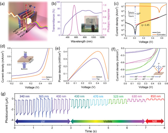
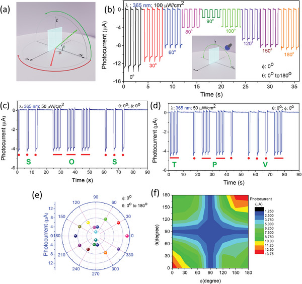
Omnidirectional photosensing is crucial in optoelectronic devices, enabling a wide field of view (wFoV) and leveraging potential applications for the Internet of Things in sensors, light fidelity, and photocommunication. The wFoV helps overcome the limitations of line-of-sight communication, and transparent photodetection becomes highly desirable as it enables the capture of optical information from various angles. Therefore, developing a photoelectric device with a 360° wFoV, ultra sensitivity to photons, power generation, and transparency is of utmost importance. This study utilizes a heterojunction of van der Waals SnS with Ga2 O3 to fabricate a transparent photovoltaic (TPV) device showing a 360° wFoV with bifacial onsite power production. SnS/Ga2 O3 heterojunction preparation consists of magnetron sputtering and is free from nanopatterning/nanostructuring to achieve the desired wFoV window device. The device exhibits a high average visible transmittance of 56%, generates identical power from bifacial illumination, and broadband fast photoresponse. Careful analysis of the device shows an ultra-sensitive photoinduced defect-modulated heterojunction and photocapacitance, revealed by the impedance spectroscopy, suggesting photon-flux driven charge diffusion. Leveraging the wFoV operation, the TPV embedded visual and speech photocommunication prototype demonstrated, aiming to help visually and auditory impaired individuals, promising an environmental-friendly sustainable future.
Keywords: field of view; omnidirectional; photocommunication; transparent photovoltaics; van der Waals.
© 2023 The Authors. Advanced Science published by Wiley-VCH GmbH.
Conflict of interest statement
The authors declare no conflicts of interest.
Figures


References
-
- Britnell L., Ribeiro R. M., Eckmann A., Jalil R., Belle B. D., Mishchenko A., Kim Y.‐J., Gorbachev R. V., Georgiou T., Morozov S. V., Grigorenko A. N., Geim A. K., Casiraghi C., Neto A. H. C., Novoselov K. S., Science 2013, 340, 1311. - PubMed
-
- Bernardi M., Palummo M., Grossman J. C., Nano Lett. 2013, 13, 3664. - PubMed
-
- Lopez‐Sanchez O., Lembke D., Kayci M., Radenovic A., Kis A., Nat. Nanotechnol. 2013, 8, 497. - PubMed
-
- Mak K. F., Shan J., Nat. Photonics 2016, 10, 216.
-
- Wang F., Wang Z., Shifa T. A., Wen Y., Wang F., Zhan X., Wang Q., Xu K., Huang Y., Yin L., Jiang C., He J., Adv. Funct. Mater. 2017, 27, 1603254.
Grants and funding
LinkOut - more resources
Full Text Sources