. 2023 Sep 6;3(6):687-698.
doi: 10.1021/acsmaterialsau.3c00056. eCollection 2023 Nov 8.

Phase Segregation Mechanisms in Mixed-Halide CsPb(BrxI1- x)3 Nanocrystals in Dependence of Their Sizes and Their Initial [Br]:[I] Ratios

Affiliations

Phase Segregation Mechanisms in Mixed-Halide CsPb(BrxI1- x)3 Nanocrystals in Dependence of Their Sizes and Their Initial [Br]:[I] Ratios

Hannah Funk et al. ACS Mater Au. .

Abstract

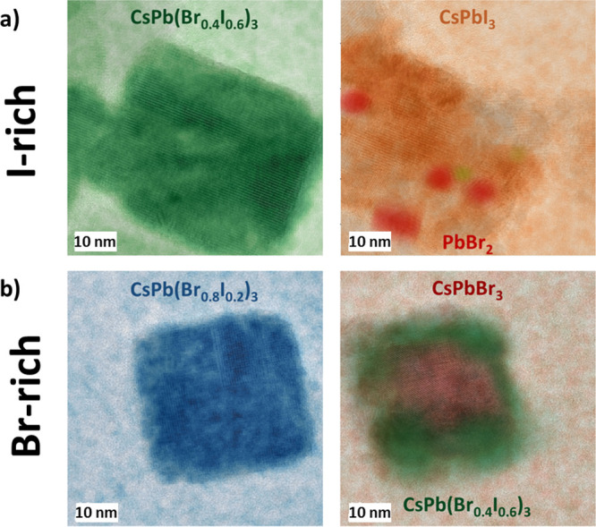
Phase segregation in inorganic CsPb(BrxI1-x)3 nanoparticles (NPs) exhibiting originally a homogeneous [Br]:[I] mixture was investigated by means of in situ transmission electron microscopy (TEM) and evaluated by using multivariate analyses. The colloidal synthesis of the NPs offers good control of the halide ratios on the nanoscale. The spatially resolved TEM investigations were correlated with integral photoluminescence measurements. By this approach, the halide-segregation processes and their spatial distributions can be described as being governed by the interaction of three partial processes: electron- and photon-irradiation-induced iodide oxidation, local differences in band gap energy, and intrinsic lattice strain. Since the oxidation can be induced by both electron-beam and light irradiation, both irradiation types can induce phase segregation in CsPb(BrxI1-x)3 compounds. This makes in situ TEM a valuable tool to monitor phase transformation in corresponding NPs and thin films on the sub-nm scale.


Conflict of interest statement

The authors declare no competing financial interest.

Figures

Figure 1
Figure 1
(a) Iodide-rich CsPb(Br0.4I0.6)3 NPs (orange) and (e) bromide-rich CsPb(Br0.8I0.2)3 NPs (yellow) dispersed in hexane. The tunability of the band gap energy is highlighted by the different colors of these solutions. (b–d) TEM images acquired at various magnifications showing CsPb(Br0.4I0.6)3 NPs as well as CsPb(Br0.8I0.2)3 NPs in (f–h). The particle side lengths vary between about 10 and 22 nm.
Figure 2
Figure 2
(a) HRTEM images acquired during the 17 min of total acquisition duration (each image 4 min); (b) characteristic diffraction patterns of the several differently orientated structures assigned to CsPb(Br0.8I0.2)3; (c) corresponding abundance maps showing no halide phase segregation, but a slow amorphization. High intensity in a pixel corresponds to high abundance of the corresponding diffractogram in that pixel. The scale bar has a length of 5 nm.
Figure 3
Figure 3
(a) PL intensity of CsPb(Br0.8I0.2)3 NPs excited with a white LED lamp over a time period of 22 min. (b) Lorentzian fit of PL peak energy indicating a blue shift of 11 meV (2.7 nm).
Figure 4
Figure 4
(a) Iodide-rich CsPb(Br0.4I0.6)3 NPs (dark red) dispersed in hexane. (b, c) TEM overview images of CsPb(Br0.4I0.6)3 NPs with side lengths from 20 to 100 nm.
Figure 5
Figure 5
Multivariate analysis of a 40 nm × 45 nm large CsPb(Br0.4I0.6)3 crystallite at position A. (a) HRTEM images acquired during 23 min of total acquisition duration, (b) characteristic diffraction patterns of most abundant structures of the upper crystallite, (c) corresponding abundance maps identified as CsPb(BrxI1–x)3 for x = 0.4, 0.25 and 0 (green, purple, and orange). As in Figure 3, a high intensity in a pixel corresponds with a high abundance of the structure in this pixel. The length of the scale bars is 10 nm.
Figure 6
Figure 6
Phases assignment at position A: (a) HRTEM after 3 min and (b) 17 min of electron beam irradiation. For exact phase assignment, the FFT of the image detail (red border) matching the diffraction pattern determined by the MSA algorithm is chosen. The exact interplanar distances are obtained from the Fourier filtered image, for initial CsPb(Br0.4I0.6)3 (green) and terminal CsPbI3 (orange). Please note that the zone axes of the crystallites are not perfectly aligned parallel to the incident electron beam.
Figure 7
Figure 7
Time series of an initially 40 nm × 50 nm large CsPb(Br0.4I0.6)3 crystallite at position B. (a) HRTEM images acquired during 14 min of total acquisition duration; (b) characteristic diffraction patterns of the most abundant structures as identified by multivariate analysis; (c) corresponding abundance maps identified as CsPb(BrxI1–x)3 for x = 0.4, 0.20, and 0.15 (green, purple, and orange). High intensity in a pixel corresponds to a high abundance of the structure in this pixel. Scale bars are 10 nm.
Figure 8
Figure 8
HRTEM image with the overlay of the I-rich ICA abundance map for (a) position A after 23 min and (b) position B after 10 min of electron-beam irradiation. In both time series, inclusions of Br-rich areas are present that can be identified as PbBr2. (c) PL peak intensity of initial CsPb(Br0.4I0.6)3 excited with a 409 nm diode laser measured over 1 min. The initial peak red shifts from 1.93 eV (645 nm) correspond to a [Br]:[I] ratio of [40]:[60] toward a stable value of about 1.77 eV (700 nm) corresponding to a ratio of [0]:[100].
Figure 9
Figure 9
Halide segregation in (a) I-rich and (b) Br-rich crystallites. While the I-rich initial crystallite segregates into CsPbI3 with Br-rich inclusions, the Br-rich initial crystallite segregates into CsPbBr3 a core and an iodide-richer phase at the edges.
Figure 10
Figure 10
Schematics of proposed mechanism for halide phase segregation in initially I-rich and Br-rich LHP.

References

    1. Egger D. A.; Bera A.; Cahen D.; Hodes G.; Kirchartz T.; Kronik L.; Lovrincic R.; Rappe A. M.; Reichman D. R.; Yaffe O. What Remains Unexplained about the Properties of Halide Perovskites?. Adv. Mater. 2018, 30, 1800691.10.1002/adma.201800691. - DOI - PubMed
    1. Saliba M.; Correa-Baena J. P.; Grätzel M.; Hagfeldt A.; Abate A. Perovskite Solar Cells: From the Atomic Level to Film Quality and Device Performance. Angew. Chem., Int. Ed. 2018, 57, 2554–2569. 10.1002/anie.201703226. - DOI - PubMed
    1. NREL . Interactive Best Research-Cell Efficiency Chart, https://www.nrel.gov/pv/interactive-cell-efficiency.html (accessed Aug 28, 2023).
    1. Al-Ashouri A.; Köhnen E.; Li B.; Magomedov A.; Hempel H.; Caprioglio P.; Márquez J. A.; Morales Vilches A. B.; Kasparavicius E.; Smith J. A.; Phung N.; Menzel D.; Grischek M.; Kegelmann L.; Skroblin D.; Gollwitzer C.; Malinauskas T.; Jošt M.; Matič G.; Rech B.; Schlatmann R.; Topič M.; Korte L.; Abate A.; Stannowski B.; Neher D.; Stolterfoht M.; Unold T.; Getautis V.; Albrecht S. Monolithic Perovskite/Silicon Tandem Solar Cell with >29% Efficiency by Enhanced Hole Extraction. Science 2020, 370, 1300–1309. 10.1126/science.abd4016. - DOI - PubMed
    1. Hoke E. T.; Slotcavage D. J.; Dohner E. R.; Bowring A. R.; Karunadasa H. I.; McGehee M. D. Reversible Photo-Induced Trap Formation in Mixed-Halide Hybrid Perovskites for Photovoltaics. Chem. Sci. 2015, 6, 613–617. 10.1039/C4SC03141E. - DOI - PMC - PubMed