

Proximity induced band gap opening in topological-magnetic heterostructure (Ni80Fe20/p-TlBiSe2/p-Si) under ambient condition
- PMID: 38097647
- PMCID: PMC10721863
- DOI: 10.1038/s41598-023-49004-5
Proximity induced band gap opening in topological-magnetic heterostructure (Ni80Fe20/p-TlBiSe2/p-Si) under ambient condition
Abstract
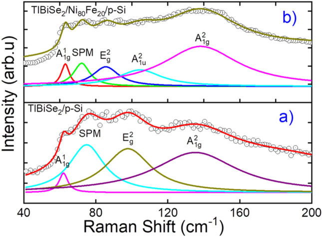
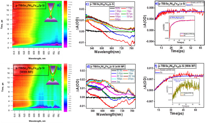
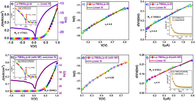
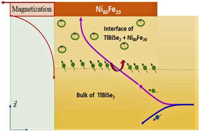
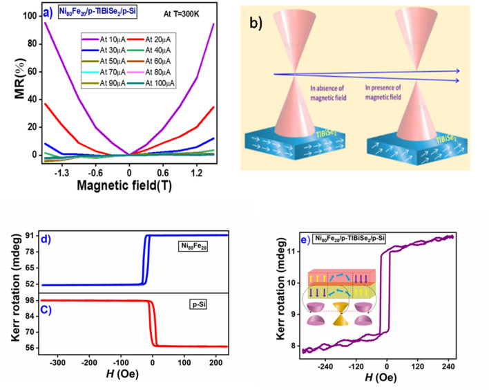
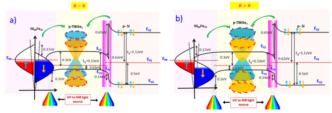
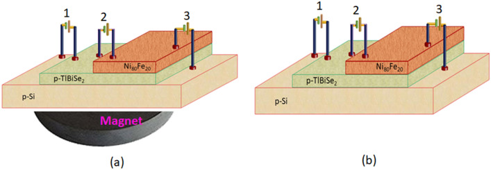
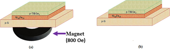
The broken time reversal symmetry states may result in the opening of a band gap in TlBiSe2 leading to several interesting phenomena which are potentially relevant for spintronic applications. In this work, the quantum interference and magnetic proximity effects have been studied in Ni80Fe20/p-TlBiSe2/p-Si (Magnetic/TI) heterostructure using physical vapor deposition technique. Raman analysis shows the symmetry breaking with the appearance of A21u mode. The electrical characteristics are investigated under dark and illumination conditions in the absence as well as in the presence of a magnetic field. The outcomes of the examined device reveal excellent photo response in both forward and reverse bias regions. Interestingly, under a magnetic field, the device shows a reduction in electrical conductivity at ambient conditions due to the crossover of weak localization and separation of weak antilocalization, which are experimentally confirmed by magnetoresistance measurement. Further, the photo response has also been assessed by the transient absorption spectroscopy through analysis of charge transfer and carrier relaxation mechanisms. Our results can be beneficial for quantum computation and further study of topological insulator/ferromagnet heterostructure and topological material based spintronic devices due to high spin orbit coupling along with dissipationless conduction channels at the surface states.
© 2023. The Author(s).
Conflict of interest statement
The authors declare no competing interests.
Figures
Similar articles
-
Effect of an external/internal magnetic field on the photocurrent in Py-topological insulator heterojunction Ni80Fe20/TI (Bi2Te3/Bi2Se3/Bi2Te2Se)/p-Si devices.Phys Chem Chem Phys. 2024 Jun 12;26(23):16708-16718. doi: 10.1039/d4cp01557f. Phys Chem Chem Phys. 2024. PMID: 38814090
-
Magnetic-Proximity-Induced Efficient Charge-to-Spin Conversion in Large-Area PtSe2/Ni80Fe20 Heterostructures.Nano Lett. 2023 Dec 27;23(24):11925-11931. doi: 10.1021/acs.nanolett.3c04060. Epub 2023 Dec 13. Nano Lett. 2023. PMID: 38088819
-
Proximity-induced magnetism and an anomalous Hall effect in Bi2Se3/LaCoO3: a topological insulator/ferromagnetic insulator thin film heterostructure.Nanoscale. 2018 May 31;10(21):10041-10049. doi: 10.1039/c8nr02083c. Nanoscale. 2018. PMID: 29774918
-
Magnetic Topological Insulator Heterostructures: A Review.Adv Mater. 2023 Jul;35(27):e2102427. doi: 10.1002/adma.202102427. Epub 2021 Oct 19. Adv Mater. 2023. PMID: 34665482 Review.
-
Recent Progress in Proximity Coupling of Magnetism to Topological Insulators.Adv Mater. 2021 Aug;33(33):e2007795. doi: 10.1002/adma.202007795. Epub 2021 Jun 29. Adv Mater. 2021. PMID: 34185344 Review.
References
LinkOut - more resources
Full Text Sources
Miscellaneous
