. 2023 Dec 13;13(24):3127.
doi: 10.3390/nano13243127.

Domain Growth in Polycrystalline Graphene

Affiliations

Domain Growth in Polycrystalline Graphene

Zihua Liu et al. Nanomaterials (Basel). .

Abstract

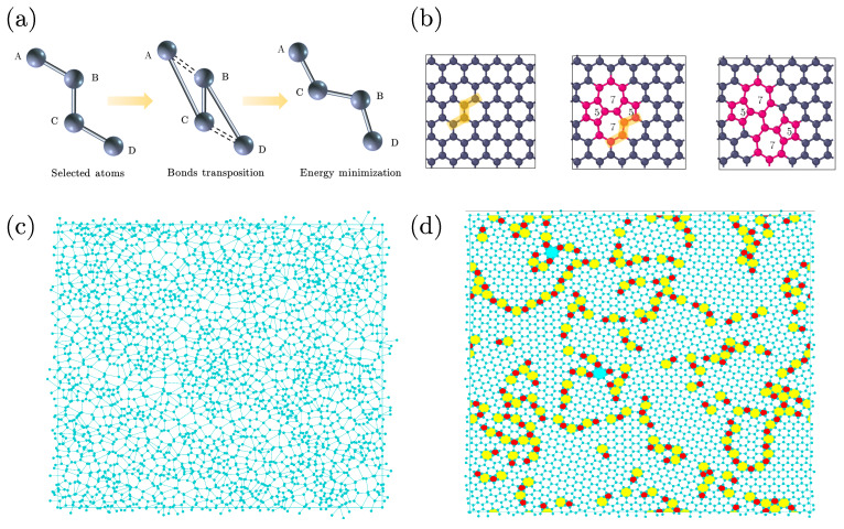
Graphene is a two-dimensional carbon allotrope which exhibits exceptional properties, making it highly suitable for a wide range of applications. Practical graphene fabrication often yields a polycrystalline structure with many inherent defects, which significantly influence its performance. In this study, we utilize a Monte Carlo approach based on the optimized Wooten, Winer and Weaire (WWW) algorithm to simulate the crystalline domain coarsening process of polycrystalline graphene. Our sample configurations show excellent agreement with experimental data. We conduct statistical analyses of the bond and angle distribution, temporal evolution of the defect distribution, and spatial correlation of the lattice orientation that follows a stretched exponential distribution. Furthermore, we thoroughly investigate the diffusion behavior of defects and find that the changes in domain size follow a power-law distribution. We briefly discuss the possible connections of these results to (and differences from) domain growth processes in other statistical models, such as the Ising dynamics. We also examine the impact of buckling of polycrystalline graphene on the crystallization rate under substrate effects. Our findings may offer valuable guidance and insights for both theoretical investigations and experimental advancements.

Keywords: Monte Carlo dynamics; disordered materials; domain growth; grain boundary; polycrystalline graphene.


Conflict of interest statement

The authors declare no conflict of interest.

Figures

Figure 1
Figure 1
(a) Elementary move in the structural evolution of polycrystalline graphene, also known as a bond transposition. In a string of four carbon atoms A-B-C-D, bonds A-B and C-D are replaced by bonds A-C and B-D, leaving the central bond, B-C, untouched. (b) Left panel: if bond transposition occurs in crystalline graphene, it results in two oppositely oriented pairs of 5–7 rings. Right panel: if bond transposition occurs in the immediate vicinity of a 5–7 pair, it effectively displaces sideways.The atoms marked in orange are selected for bond transposition. (c) Visualization of an initial sample, created from a Voronoi network as described in the text. We note that the network is disordered and homogeneous, with at most tiny crystalline regions. (d) Same network after structural relaxation with 9×10⁴ proposed bond transitions, when crystalline regions have appeared. In this figure, 5-, 7- and 8-fold rings are marked in different colors.
Figure 2
Figure 2
Comparison of the normalized radial distribution function g(r) of our generated sample and experiment at comparable defect density. The two curves match very well, up to about the first ten peaks [37].
Figure 3
Figure 3
Time evolution of the distribution of (a) the bond angles and (b) the bond lengths in planar samples of graphene. With increasing simulation times, both distributions become narrower. (c) Time evolution of the radial distribution function. With increasing simulation time, the peaks at longer distance become increasingly pronounced. (d) Density of defects (5 and 7 rings) as a function of simulation time. The decay can be well fitted by a power-law decay t1/3 (solid line).
Figure 4
Figure 4
Total energy as a function of the number of defects (pairs of 5 and 7 rings) in planar graphene. The data can be well fitted with a linear relation: E=1.75x+7.86. As a reference, a single SW defect consists of two such pairs and would thus correspond to a defect formation energy of 3.5 eV.
Figure 5
Figure 5
Analysis of the orientation of the hexagons in the lattice —10 10−10 structure. (a) Normalized correlation function Csori of the orientations as defined in Equation (5), as a function of distance r, for various times. The data show a linear trend if (ln(Csori)) is plotted as a function of distance r in a double-logarithmic plot, indicating that correlation function Csori decays as a stretched exponential. (b) Histogram of the hexagon orientations at different times. While the crystalline regions grow in time, these histograms become increasingly rugged. (c) Evolution of the maps of hexagon orientations. Some regions grow (while conserving their orientation) at the expense of other regions that shrink and sometimes disappear.
Figure 6
Figure 6
(a) A polycrystalline graphene with 9800 atoms; 36 crystal phases are identified by using the graph clustering algorithm. Green, yellow and blue boxes represent three different kinds of defect structures; details see in the text. (b) The average domain area changes in time, which approximately scales as a power law with a 1/3 exponent. (c) Movement of a defect island from the inside domain to thr grain boundary, showing the diffusive behavior of the defect.
Figure 7
Figure 7
(a) A brief schematic diagram illustrating the growth of buckled polycrystalline graphene on a substrate. (b) Defect density of buckled polycrystalline graphene growing on various substrates divided by t1/3 (the decay rate in the flat case) over time. The inner figure is plotted on a double-logarithmic scale, demonstrating that the buckling of polycrystalline graphene slows down the crystallization rate. All samples are evolved starting from an initial configuration with 20% defect density. Since a well-crystallized sample leads to a higher buckling height Δz, which counteracts the suppression of substrate, the difference is weak for various values of K (eV Å2).

Similar articles

References

    1. Song N., Gao Z., Li X. Tailoring nanocomposite interfaces with graphene to achieve high strength and toughness. Sci. Adv. 2020;6:eaba7016. doi: 10.1126/sciadv.aba7016. - DOI - PMC - PubMed
    1. Zhang P., Ma L., Fan F., Zeng Z., Peng C., Loya P.E., Liu Z., Gong Y., Zhang J., Zhang X., et al. Fracture toughness of graphene. Nat. Commun. 2014;5:3782. doi: 10.1038/ncomms4782. - DOI - PubMed
    1. Shekhawat A., Ritchie R.O. Toughness and strength of nanocrystalline graphene. Nat. Commun. 2016;7:10546. doi: 10.1038/ncomms10546. - DOI - PMC - PubMed
    1. Lee C., Wei X., Kysar J.W., Hone J. Measurement of the elastic properties and intrinsic strength of monolayer graphene. Science. 2008;321:385–388. doi: 10.1126/science.1157996. - DOI - PubMed
    1. Zandiatashbar A., Lee G.H., An S.J., Lee S., Mathew N., Terrones M., Hayashi T., Picu C.R., Hone J., Koratkar N. Effect of defects on the intrinsic strength and stiffness of graphene. Nat. Commun. 2014;5:3186. doi: 10.1038/ncomms4186. - DOI - PubMed

LinkOut - more resources