A Strategy for Tuning Electron-Phonon Coupling and Carrier Cooling in Lead Halide Perovskite Nanocrystals
- PMID: 38133031
- PMCID: PMC10745929
- DOI: 10.3390/nano13243134
A Strategy for Tuning Electron-Phonon Coupling and Carrier Cooling in Lead Halide Perovskite Nanocrystals
Abstract
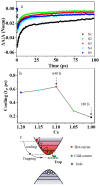
Perovskites have been recognized as a class of promising materials for optoelectronic devices. We intentionally include excessive Cs+ cations in precursors in the synthesis of perovskite CsPbBr3 nanocrystals and investigate how the Cs+ cations influence the lattice strain in these perovskite nanocrystals. Upon light illumination, the lattice strain due to the addition of alkali metal Cs+ cations can be compensated by light-induced lattice expansion. When the Cs+ cation in precursors is about 10% excessive, the electron-phonon coupling strength can be reduced by about 70%, and the carrier cooling can be slowed down about 3.5 times in lead halide perovskite CsPbBr3 nanocrystals. This work reveals a new understanding of the role of Cs+ cations, which take the A-site in ABX3 perovskite and provide a new way to improve the performance of perovskites and their practical devices further.
Keywords: carrier cooling; electron–phonon coupling; light–induced lattice expansion; perovskites.
Conflict of interest statement
The authors declare no conflict of interest.
Figures


Similar articles
-
Harnessing Hot Phonon Bottleneck in Metal Halide Perovskite Nanocrystals via Interfacial Electron-Phonon Coupling.Nano Lett. 2020 Jun 10;20(6):4610-4617. doi: 10.1021/acs.nanolett.0c01452. Epub 2020 May 20. Nano Lett. 2020. PMID: 32421338
-
Charge-Carrier Dynamics of Lead-Free Halide Perovskite Nanocrystals.Acc Chem Res. 2019 Nov 19;52(11):3188-3198. doi: 10.1021/acs.accounts.9b00422. Epub 2019 Oct 30. Acc Chem Res. 2019. PMID: 31664815
-
Stacking Effects on Electron-Phonon Coupling in Layered Hybrid Perovskites via Microstrain Manipulation.ACS Nano. 2020 May 26;14(5):5806-5817. doi: 10.1021/acsnano.0c00907. Epub 2020 Apr 23. ACS Nano. 2020. PMID: 32293867
-
Doping and ion substitution in colloidal metal halide perovskite nanocrystals.Chem Soc Rev. 2020 Jul 21;49(14):4953-5007. doi: 10.1039/c9cs00790c. Chem Soc Rev. 2020. PMID: 32538382 Review.
-
Research progress of ABX3-type lead-free perovskites for optoelectronic applications: materials and devices.Phys Chem Chem Phys. 2022 Nov 23;24(45):27585-27605. doi: 10.1039/d2cp02451a. Phys Chem Chem Phys. 2022. PMID: 36373364 Review.
References
-
- Tsai H., Shrestha S., Vilá R.A., Huang W., Liu C., Hou C.-H., Huang H.-H., Wen X., Li M., Wiederrecht G., et al. Bright and stable light-emitting diodes made with perovskite nanocrystals stabilized in metal–organic frameworks. Nat. Photonics. 2021;15:843–849. doi: 10.1038/s41566-021-00857-0. - DOI
-
- Feng J.G., Gong C., Gao H.F., Wen W., Gong Y.J., Jiang X.Y., Zhang B., Wu Y.C., Wu Y.S., Fu H.B., et al. Single-crystalline layered metal-halide perovskite nanowires for ultrasensitive photodetectors. Nat. Electron. 2018;1:404–410. doi: 10.1038/s41928-018-0101-5. - DOI
-
- Protesescu L., Yakunin S., Bodnarchuk M.I., Krieg F., Caputo R., Hendon C.H., Yang R.X., Walsh A., Kovalenko M.V. Nanocrystals of Cesium Lead Halide Perovskites (CsPbX3, X = Cl, Br, and I): Novel Optoelectronic Materials Showing Bright Emission with Wide Color Gamut. Nano Lett. 2015;15:3692–3696. doi: 10.1021/nl5048779. - DOI - PMC - PubMed
LinkOut - more resources
Full Text Sources

