Review
. 2023 Dec 15;13(24):3148.
doi: 10.3390/nano13243148.

3D Printed Integrated Sensors: From Fabrication to Applications-A Review

Affiliations
Review

3D Printed Integrated Sensors: From Fabrication to Applications-A Review

Md Sahid Hassan et al. Nanomaterials (Basel). .

Abstract

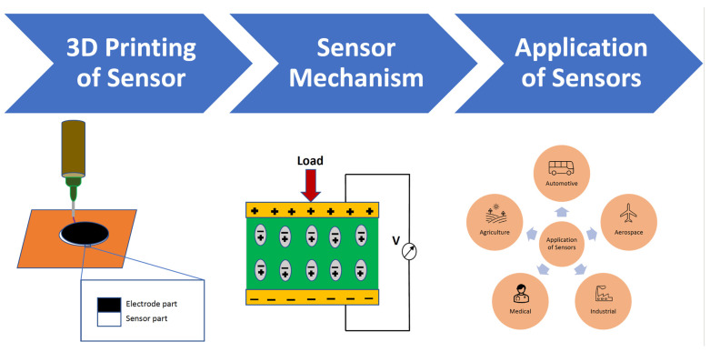
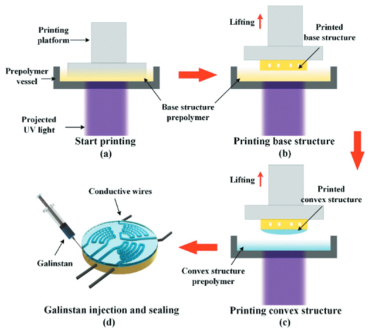
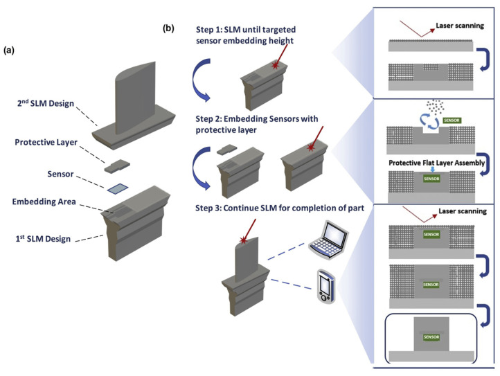
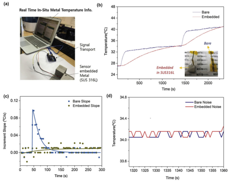
The integration of 3D printed sensors into hosting structures has become a growing area of research due to simplified assembly procedures, reduced system complexity, and lower fabrication cost. Embedding 3D printed sensors into structures or bonding the sensors on surfaces are the two techniques for the integration of sensors. This review extensively discusses the fabrication of sensors through different additive manufacturing techniques. Various additive manufacturing techniques dedicated to manufacture sensors as well as their integration techniques during the manufacturing process will be discussed. This review will also discuss the basic sensing mechanisms of integrated sensors and their applications. It has been proven that integrating 3D printed sensors into infrastructures can open new possibilities for research and development in additive manufacturing and sensor materials for smart goods and the Internet of Things.

Keywords: 3D printing; additive manufacturing; embedded sensor; sensor integration.


Conflict of interest statement

The authors declare no conflict of interest.

Figures

Figure 1
Figure 1
Basic sensor fabrication technique, sensing mechanism and applications.
Figure 2
Figure 2
Schematic illustration of three common transduction methods and representative devices: (a) piezoresistivity (b) capacitance and (c) piezoelectricity [64]. Copyright 2015, Wiley Online Library.
Figure 3
Figure 3
Process schematic of Fused Filament Fabrication (FFF) [80]. Copyright 2017, Elsevier.
Figure 4
Figure 4
Coordinate system and mode response directions for a FFF piezoelectric PVDF film (Left), and single-process FFF dynamic sensor design with selected dimensions (Right) [80]. Copyright 2021, Elsevier.
Figure 5
Figure 5
(a) Negative molds design; (b) 3D printed mold via SLA technology; (c) trenches and electrode patterns filled with PDMS conductive ink; (d) electrodes after Au sputtering; (e) electrodes after Au electroplating; (f) Au (left) and carbon (right) full chip [83]. Copyright 2015, Elsevier.
Figure 6
Figure 6
(A) Schematic presentation of the 3D-printing procedure for fabricating the cell-on-a-chip device using a dual extruder 3D printer. (B) The dimensions of the 3D-printed cell-on-a-chip device (in cm). (C) Photograph of the 3D-printed device [81]. Copyright 2019, Elsevier.
Figure 7
Figure 7
Indirect fabrication of sensors via printed channels: (a) sensor body with support material in channels space, (b) removal of supports to leave empty channels, (c) piezoresistive ink injections or direct ink writing [54]. Copyright 2018, MDPI.
Figure 8
Figure 8
Examples of multi-material printing via Vat Photopolymerization technology: (a) manually switching vats(I) free surface and (II) constrained surface SLA system, (b) manually changing resins by injecting layer-by-layer [85]. Copyright 2021, American Chemical Society.
Figure 9
Figure 9
Step by Step fabrication process of tactile sensor by Wang et al. [86]. Copyright 2021, Taylor & Francis Online.
Figure 10
Figure 10
Sensing performance of tactile sensors: (a) resistance change under different loading forces, (b) resistance change under different loading frequencies, (c) 200 cyclic loading and unloading, (d) cyclic heating and cooling tests [46]. Copyright 2021, Taylor & Francis Online.
Figure 11
Figure 11
(a) CAD model of the demonstrator with dedicated cavity design for integration of EC sensors; (b) schematic representation of the demonstrator prior to crack initiation; (c) schematic representation of the demonstrator showing the crack propagating towards the embedded sensor [104]. Copyright 2021, Springer Link.
Figure 12
Figure 12
Sensor integration process for EC sensors: (a) powder removal, insertion of heat shrink tubes as wire protection and leading of wires through heat shrink tubes; (b) integration of the EC sensor into the cavity; (c) LPBF test specimens with soldered cables, ready to be tested [104]. Copyright 2021, Springer Link.
Figure 13
Figure 13
Schematic of sensor embedding selective laser melting (SE-SLM). (a) Design configuration of parts for the intermittent SLM process. (b) Three primary steps and details of the SE-SLM process [57]. Copyright 2020, Elsevier.
Figure 14
Figure 14
Validation of SE-SLM-processed temperature sensor operation by comparison with a bare temperature sensor. (a) Data reading set-up for monitoring the in-situ temperature of SE-SLM SUS316L. (b) Temperature profile comparison (c) Temperature increment slope profile (d) Noise level comparison [57]. Copyright 2020, Elsevier.
Figure 15
Figure 15
PCB-based IC component embedding in metal. (a) Setup for data reading from IC chip embedded in metal component. (b) IC chip-embedded Inconel 718 turbine vane. (c) Remote wireless monitoring of turbine vane temperature. (df) Recorded acceleration data for each axis vibration input ((d) X-axis, (e) Y-axis, and (f) Z-axis) [57]. Copyright 2020, Elsevier.
Figure 16
Figure 16
Image of laser powered DED process [107]. Copyright 2019, 3D natives.
Figure 17
Figure 17
(A) MultiJet and (B) PolyJet printing schematics [110].
Figure 18
Figure 18
(i) The electric charge of the piezoelectric PVDF effect results from a deformation of the crystal lattice by changing the distance d when applying the pressure, producing a dipole moment. (ii) The results of PVDF microfluidic experimental data acquisition by LabVIEW software. (a) The capacitance values with the air flow impulses at differential pressures. (b) The voltages transfor-mation from capacitance by a charge amplifier. (c) The different frequency amplitudes with flow rates. (d) The output amplitude of the flow rates of frequency response versus the flow rate under different curvature radii [124], Copyright 2008, IEEE.
Figure 19
Figure 19
SEM image of 3D printed accelerometer by Pagliano et al. [126], Copyright 2022, Springer Nature.
Figure 20
Figure 20
3D printed MWCNT-PDMS material patterns on soft substrates: (a) 3D printed film with extreme flexibility and bendability which shows that the sensor can be attached to non-conformal surfaces in practical applications; (b) 3D printed stretchable serpentine shape; (c) 3D printed grid forming 576 “taxels”; (d) printed MWCNT-PDMS composite on a non-conformal surface by Fekiri et al. [131], Copyright 2020, MDPI.
Figure 21
Figure 21
Schematic of the 3D printed microfluidic device [59]. Copyright 2017, Elsevier.
Figure 22
Figure 22
Schematic of the microchannels that form the virtual impactor in the miniature sensor [141]. Copyright 2018, AMA.
Figure 23
Figure 23
Tactile sensor phalanx structure of robotic hand; (a) whole phalanx structure, (b) fabrication procedure, (c) 3D printing via cold extrusion [143]. Copyright 2019, Wiley Online Library.
Figure 24
Figure 24
3D printed e-skin with incorporated tactile sensor [47]. Copyright 2021, Elsevier.
Figure 25
Figure 25
Illustration of the dengue virus serotype biosensor prototype assembly and components. (a) The prototype consists of the Fluidic chip component. (b) The cross-section illustrates the press structure that pushes the reaction zone (yellow mesh area) up against the reaction cover (white mesh area) [148]. Copyright 2021, Elsevier.
Figure 26
Figure 26
Specificity of RNA toehold switches for dengue virus serotype detection in cell-free reactions. The bar graphs were generated from the mean and ±SD (n = 3) of the color intensity from the cell-free reactions containing the RNA toehold switches (DENV-1 to DENV-4) that were exposed to 5 μM Trigger-DENV-1 to Trigger DENV-4 and HPV16 (negative control) [148]. Copyright 2021, Elsevier.
Figure 27
Figure 27
Characterization of a 3D integrated electrical oscillator. (a) Equivalent circuit of Colpitts oscillator. (b) Schematic of the 3D integrated electrical oscillator. (c) Fabrication procedure for the embedded oscillator. (d) Image of the printed 3D oscillator. (e) LTspice simulation of AC signal produced by Colpitts circuits. (f) Experimental output from the 3D-shaped oscillator [150]. Copyright 2021, Elsevier.
Figure 28
Figure 28
(a) Performance of the 3D integrated neuromorphic system for sensing various K+ ion concentrations. (b) Normalization of output from the fabricated 3D integrated neuromorphic sytem [150]. Copyright 2021, Elsevier.

References

    1. Wang C.H., Liu Y., Desmulliez M., Richardson A. Integrated sensors for health monitoring in advanced electronic systems; Proceedings of the 2009 4th International Design and Test Workshop (IDT); Riyadh, Saudi Arabia. 15–17 November 2009; pp. 1–6.
    1. Qiu K., Zhao Z., Haghiashtiani G., Guo S.-Z., He M., Su R., Zhu Z., Bhuiyan D.B., Murugan P., Meng F., et al. 3D Printed Organ Models with Physical Properties of Tissue and Integrated Sensors. Adv. Mater. Technol. 2018;3:1700235. doi: 10.1002/admt.201700235. - DOI - PMC - PubMed
    1. Petrie C.M., Leonard D.N., Yang Y., Trammell M.P., Jolly B.C., Terrani K. Embedment of Sensors in Ceramic Structures. Oak Ridge National Lab. (ORNL); Oak Ridge, TN, USA: 2019.
    1. Zaman S., Leyva A., Hassan S., Valladolid A., Herrera N.E., Gomez S.G., Mahmud S., Tucker D., Haynes C., Lin Y. Implementation of Smart Materials for Actuation of Traditional Valve Technology for Hybrid Energy Systems. Actuators. 2023;12:131. doi: 10.3390/act12030131. - DOI
    1. Senesky D.G., Jamshidi B., Cheng K.B., Pisano A.P. Harsh Environment Silicon Carbide Sensors for Health and Performance Monitoring of Aerospace Systems: A Review. IEEE Sens. J. 2009;9:1472–1478. doi: 10.1109/JSEN.2009.2026996. - DOI

LinkOut - more resources