. 2024 Jan 2;15(1):185.
doi: 10.1038/s41467-023-44200-3.

Elastocapillarity-driven 2D nano-switches enable zeptoliter-scale liquid encapsulation

Affiliations

Elastocapillarity-driven 2D nano-switches enable zeptoliter-scale liquid encapsulation

Nathan Ronceray et al. Nat Commun. .

Abstract

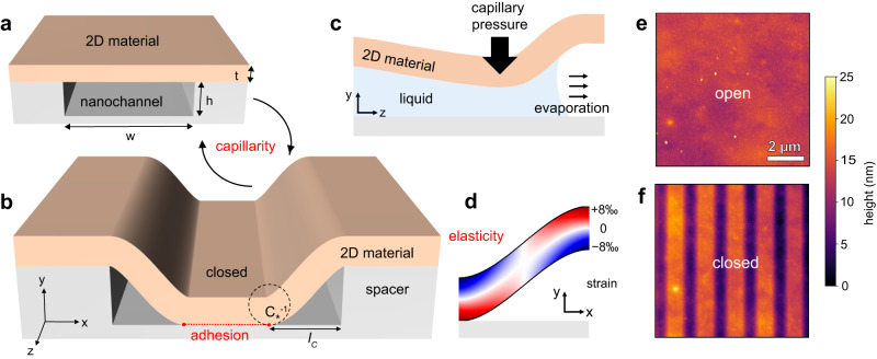
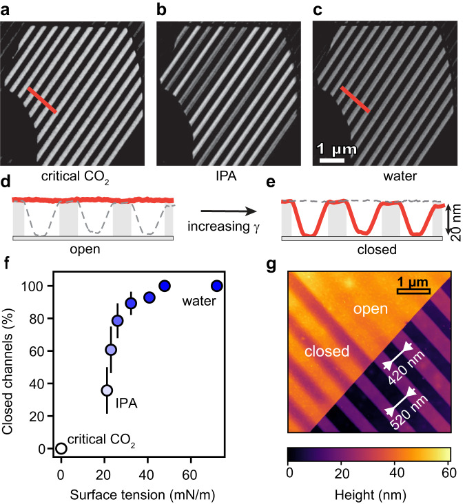
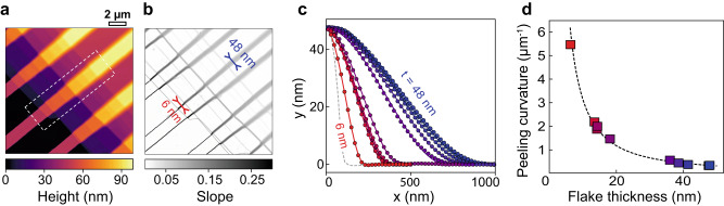
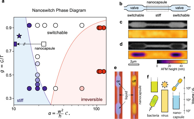
Biological nanostructures change their shape and function in response to external stimuli, and significant efforts have been made to design artificial biomimicking devices operating on similar principles. In this work we demonstrate a programmable nanofluidic switch, driven by elastocapillarity, and based on nanochannels built from layered two-dimensional nanomaterials possessing atomically smooth surfaces and exceptional mechanical properties. We explore operational modes of the nanoswitch and develop a theoretical framework to explain the phenomenon. By predicting the switching-reversibility phase diagram-based on material, interfacial and wetting properties, as well as the geometry of the nanofluidic circuit-we rationally design switchable nano-capsules capable of enclosing zeptoliter volumes of liquid, as small as the volumes enclosed in viruses. The nanoswitch will find useful application as an active element in integrated nanofluidic circuitry and could be used to explore nanoconfined chemistry and biochemistry, or be incorporated into shape-programmable materials.


Conflict of interest statement

The authors declare no competing interests.

Figures

Fig. 1
Fig. 1. Elastocapillarity-switched adhesion in nanochannels.
a Sketch of a nanochannel device in the stiff configuration. b Nanochannel in its caved-in state, where the top flake adheres to the substrate. C is the peeling curvature parameter and C1 thus corresponds to the radius of curvature (dashed circle). c Upon drying the channel, capillary pressure triggers the caving-in of the top wall. d Calculated strain map in the bent cross-section using blue for compressive and red for tensile strain. The strain color scale refers to device D1, presented in (e, f) AFM (Atomic Force Microscopy) height maps of hBN/Gr/SiO2 nanochannels in their stiff and caved-in configurations, respectively.
Fig. 2
Fig. 2. Visualizing and quantifying the nanoswitch optically and with Atomic Force Microscopy (AFM).
ac Optical micrographs of nanochannel device D2 after drying with different liquids. The bright and dark gray lines correspond to open or collapsed nanochannels, respectively. d, e Correlating the optical image to AFM profiles of channels after varying drying conditions. f Caved-in channels in the thick top region were optically counted as in (b) after drying with liquids of different surface tensions. IPA/water mixtures were used to interpolate the surface tension from 21 to 72 mN/m. Error bars correspond to standard deviations over three wetting/drying measurements. g Visualizing the width threshold for caving under capillary pressure: AFM map of hBN/Gr/SiO2 device D3 with channels of two different widths, switched by water capillarity stimulus. The bottom-right half (dark) of the image presents open spacers, with h=17nm high graphene sidewalls. Top-left (bright) part shows the same spacers topped with t=22nm thick hBN top wall, defining the nanochannels—the upper set of channels is open, while the lower is collapsed.
Fig. 3
Fig. 3. Adhesion/stiffness analysis of closed channels in device D4, obtained by exfoliating a terraced WS2 crystal on SiO2 spacers.
a Atomic Force Microscopy height map of the collapsed nanochannels with varying top wall thickness t ranging from 6 to 48 nm. b Slope extracted from the height map showing that the width of the transition zone increases with the crystal thickness. c Height profiles extracted along lines in the white dashed zone of (a) following the lines shown in (b). The dots are experimental points, and the solid black lines are the best fit to the polynomial profile obtained in our model. The top layer thickness was subtracted from the profiles. The x and y axis follow the convention defined in Fig. 1. d Peeling curvature C extracted from the profiles in (c), as a function of the crystal thickness. The dashed line is the best fit to a power law C~tQ/2, yielding Q=2.88±0.08.
Fig. 4
Fig. 4. Generalization and application of the nanoswitch.
a Universal nanoswitch phase diagram. The dimensionless parameter α=w2C/h defines the channel geometry-dependent flexibility, and g=G/Γ defines the material wettability/adhesion ratio. Markers represent experiments for different geometry, solvents, and materials. Different regions in the parameter space are color-coded. For low α, channels do not cave in upon liquid removal; this is the stiff region (blue). For high α and low g, the channels irreversibly collapse on the substrate (red). The remaining space is the switchable region, where channels undergo on/off transitions during wetting/drying (white). The star denotes the mechanical stability upper limit empirically established for atomically thin 2D nanoslits. Squares denote parts of the nanocapsule: the open square is the switch part, and the blue square is for the container (off-scale, real value for container is g4). b A sketch of a self-sealing nanocapsule, consisting of a narrow stiff nanocontainer, delimited by two switchable valves. c Implementation of the nanocapsule, visualized in open configuration by optical microscopy (top) and AFM (bottom). d The same nanocapsule in closed state, where IPA removal switches off the valves, sealing the nanocontainer with zeptoliter volume. e Color-scale optical image of an open nanocapsule filled with liquid (blue) with open nanoswitch gates (left). The same nanocapsule with closed off nanoswitch gates, sealing in the ~100 zL of liquid inside (right). f Comparison of the range of volumes encapsulated inside bacteria, viruses and different nano-capsules implemented in this work.

Similar articles

Cited by

References

    1. Coste B, et al. Piezo proteins are pore-forming subunits of mechanically activated channels. Nature. 2012;483:176–181. doi: 10.1038/nature10812. - DOI - PMC - PubMed
    1. McEvoy, M. A. & Correll, N. Materials that couple sensing, actuation, computation, and communication. Science347, 1261689 (2015). - PubMed
    1. Bocquet L. Nanofluidics coming of age. Nat. Mater. 2020;19:254–256. doi: 10.1038/s41563-020-0625-8. - DOI - PubMed
    1. Geim AK. Exploring two-dimensional empty space. Nano Lett. 2021;21:6356–6358. doi: 10.1021/acs.nanolett.1c02591. - DOI - PubMed
    1. Blees MK, et al. Graphene kirigami. Nature. 2015;524:204–207. doi: 10.1038/nature14588. - DOI - PubMed