. 2024 Jan 3;14(1):434.
doi: 10.1038/s41598-023-50698-w.

Quasi-instantaneous materials processing technology via high-intensity electrical nano pulsing

Affiliations

Quasi-instantaneous materials processing technology via high-intensity electrical nano pulsing

Eugene A Olevsky et al. Sci Rep. .

Abstract

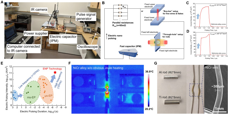
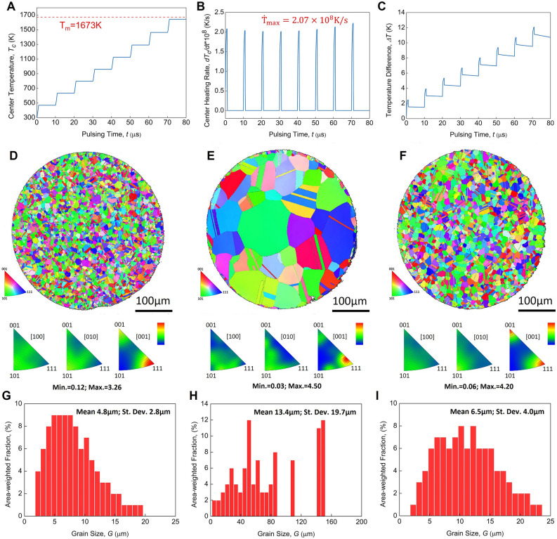
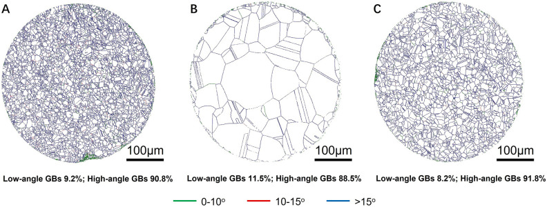
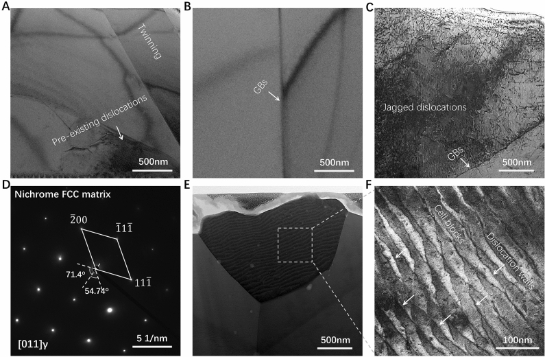
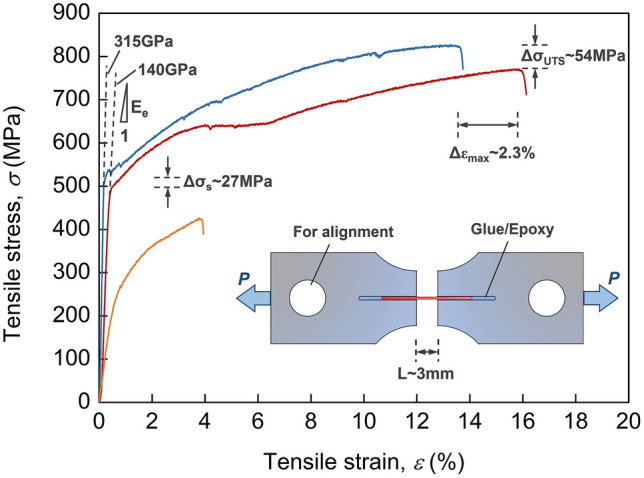
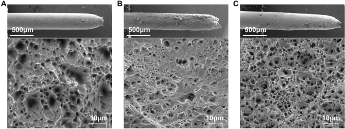
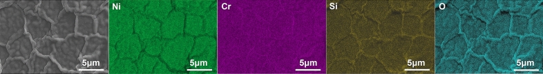
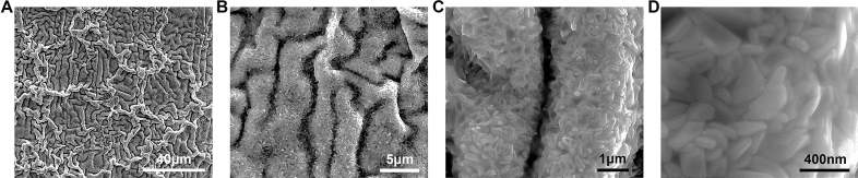
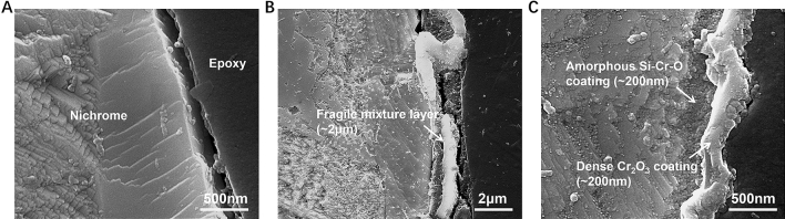
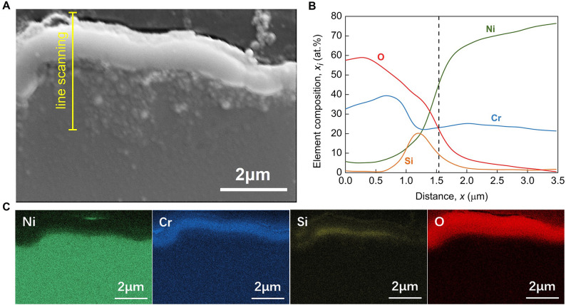
Despite many efforts, the outcomes obtained with field-assisted processing of materials still rely on long-term coupling with other electroless processes. This conceals the efficacy and the intrinsic contributions of electric current. A new device utilizing electrical nano pulsing (ENP) has been designed and constructed to bring quasi-instantaneous modifications to the micro- and nano-structure in materials. Featuring ultra-high intensity (~ 1011 A/m2) and ultra-short duration (< 1 μs), the ENP technology activates non-equilibrium structural evolutions at nanometer spatial scale and nanosecond temporal scale. Several examples are provided to demonstrate its utility far outpacing any conventional materials processing technology. The ENP technology gives a practical tool for exploring the intrinsic mechanism of electric-field effects and a pathway towards the rapid industrial manufacturing of materials with unique properties.


Conflict of interest statement

The authors declare no competing interests.

Figures

Figure 1
Figure 1
The illustration of proposed electric nano pulsing (ENP) technology. (A) Physical picture of the constructed ENP machine with all major component labeled. (B) Schematic diagram showing the electric circuit features and possible sample set up in ENP machine. (C) Example on the electric pulsing showing the current density curve (3.15 × 1010 A/m2) output by ENP machine. (D) Another example on the electric pulsing showing the current density curve (1.49 × 1011 A/m2) output by ENP machine. (E) Comparison between the proposed ENP technology and other existed electric pulsing technologies showing all-around performance improvement,,,–,–. (F) Example on the temperature map of nichrome alloy during ENP process showing no obvious temperature rise by Joule heating effect. (G) Exemplary images of some conductive materials that are subject to ENP process by different sample setups.
Figure 2
Figure 2
The simulated temperature and measured microstructure of nichrome alloy demonstrating the quasi-instantaneous and localized features of ENP processing. (A) The temperature at alloy component’s center over the pulsing time. (B) The corresponding heating rate over the pulsing time. (C) The temperature different between the alloy component’s center and the edge over the pulsing time. (D, E and F) EBSD inverse pole figures (IPF) of the cross-sections of nichrome wires. (G, H and I) Grain size distributions of nichrome wires: (D and G) raw sample, (E and H) after conventional heating, (F and I) after ENP processing.
Figure 3
Figure 3
Images showing the grain boundaries distributions and orientations in nichrome alloys. (A) Raw sample. (B) After conventional heating. (C) After ENP processing.
Figure 4
Figure 4
Bright-field TEM images showing the comparison of dislocation configurations in nichrome alloys. (A) Raw sample. (B) After conventional heating. (C) After ENP processing of two electric pulses with current density of 6.98 × 1010 A/m2, pulsing duration of 1 μs and pulsing frequency of 100 kHz. (D) Corresponding selected area electron diffraction pattern (SAED) of the FCC matrix along [011] zone axis. (E) After ENP processing of eight electric pulses with current density of 3.15 × 1010 A/m2, pulsing duration of 1 μs and pulsing frequency of 100 kHz. (F) Zoom-in image on the white dash square area showing the detailed dislocation morphology.
Figure 5
Figure 5
Engineering stress–strain curves of nichrome alloys under tensile test. raw sample (red); after ENP processing (blue) and after conventional heating (orange). The ENP processing has eight electric pulses at the current density of 3.15 × 1010 A/m2, the pulsing duration of 1 μs and the pulsing frequency of 100 kHz. The insert is a schematic diagram showing the Aluminum setup tooling for tensile test of fine alloy wire at Instron 5800 mechanical testing machine. Cylinder rods are inserted into the round holes and clamped onto the fixtures of Instron machine to obtain good alignment of alloy wires during tensile tests. Glue or epoxy (curing in vacuum) are used to mounting the two ends of alloy wires to achieve good bonding and minimize the stress concentration during tensile tests.
Figure 6
Figure 6
SEM images showing the macroscopic fracture surface and the detail ductile fracture features of nichrome alloy after different processing. (A) Raw sample. (B) After conventional heating. (C) After ENP processing. The ENP processing has the current density of 3.15 × 1010 A/m2, the pulsing duration of 1 μs and the pulsing frequency of 100 kHz. All the nichrome alloys show typical ductile fracture behavior. The fracture surface of alloy after ENP processing still has the same dense dimple structure as that of raw sample. However, conventional heating produces the loose dimple structure with partial brittle characteristics on its fracture surface, indicating an obvious properties degradation.
Figure 7
Figure 7
SEM images showing the evolution of exterior surface morphology on the nichrome alloy surface after multiple electric pulsing. This alloy was subjected to ENP processing with the current density of 3.15 × 1010 A/m2, the pulsing duration of 1 μs, the pulsing frequency of 100 kHz and the duty period of 10%. The triple hierarchical structure of nanocoating on alloy exterior surface is formed after its gradual development during ENP processing. The obvious oxidation formation is seen on alloy surface after releasing three pulses (3 μs pulsing time or 30 μs total processing time). After seven electric pluses are released in this case, only more severe oxidation formation is observed, which indicates that this triple hierarchical structure of nanocoating is instantaneously generated within 1 μs at the temperature near melting point.
Figure 8
Figure 8
The morphology of nanocoating on nichrome alloy after ENP processing. (A–D) The exterior surface morphology by SEM imaging showing the triple hierarchical structure of nanocoating on the nichrome alloy surface: (A) low-magnification view, (B) fold-like morphology at micro-scale, (C) ravine-like morphology at sub-nanoscale and (D) well-faceted crystals at nano-scale. (EH) The cross-section morphology by TEM imaging showing the double-layer ultra-thin structure of nanocoating on the nichrome alloy surface: (E) overall TEM BF images, (F and G) zoom-in TEM BF images showing the detailed structure of inner amorphous Si–Cr–O layer and outer Cr2O3 layer, (H) corresponding SAED patterns of polycrystalline Cr2O3 layer and amorphous Si–Cr–O layer. (I) TEM-EDS mapping showing the element distribution on the cross-section of this surface nanocoating, in which the white dash line indicates the position of oxidation coating.
Figure 9
Figure 9
EDS mapping showing the non-uniform element distribution on surface triple hierarchical nanocoating of nichrome alloy after ENP processing. Cr exhibits an almost indiscriminate distribution. The raised portion of folds, enriched in Si and O but lacking Ni, are possibly the GBs with a greater degree of oxidation. This hierarchical oxidation coating should be Ni-depleted, and those well-faceted nanocrystals should be almost chromium oxide (Cr2O3).
Figure 10
Figure 10
EDS measurements showing the evolution of element concentration on the surface triple hierarchical nanocoating of nichrome alloy as a function of pulsing number. The ENP processing has the current density of 3.15 × 1010 A/m2, the pulsing duration of 1 μs and the pulsing frequency of 100 kHz. Here pulsing number is corresponding to pulsing cycle, which has 10 μs processing time with 1 μs pulsing time in it. With the ENP processing ongoing, oxygen content gradually increases whilst nickel becomes depleted. Silicon and chromium stay almost constant in this case, indicating that it is mainly the chromium oxide and silicon oxide formation on nichrome alloy surface.
Figure 11
Figure 11
The exterior surface morphology by SEM imaging showing the coarse surface structure on nichrome alloy under conventional furnace at 1400 °C (melting point) for ten seconds. With the magnification increasing from figure (A) to figure (D), the spheroidization and coarsening of surface layer is clearly observed compared with ENP treated nichrome alloy, which can lead to the property degradation.
Figure 12
Figure 12
SEM images showing the cross-section view of surface oxidation coating on nichrome alloy wires etched by HCl/CuSO4 ethanol solution. (A) Raw sample. (B) After conventional heating. (C) After ENP processing. The ENP processing has the current density of 3.15 × 1010 A/m2, the pulsing duration of 1 μs and the pulsing frequency of 100 kHz. Nichrome alloy can hardly form any oxidation layer on its surface under natural conditions at room temperature. Conventional heating at 1400 °C leads to the appearance of fragile layer as expected. Excessive high temperature oxidation is generally not welcomed in metallic materials due to material loss and property damage. Indeed, the thermal oxidation of nichrome alloy by prolonged conventional heating brings unwanted Ni/Cr loss and a thick (~ 2 μm) irregular layer that significantly spalled from surface. In contrast, a dense double-layer coating with a thickness of nanometer scale is achieved by this ENP processing.
Figure 13
Figure 13
Cross-section EDS measurements on the surface of nichrome alloy under conventional furnace at 1400 °C (melting point) for ten seconds. (A) SEM image showing the location for EDS measurements. (B) EDS line scanning showing the various elements presented inside the surface oxidation layer. (C) EDS element mapping showing the formation of single-layered Cr2O3/NiO/SiO2 mixture on surface.

References

    1. Lu K. Stabilizing nanostructures in metals using grain and twin boundary architectures. Nat. Rev. Mater. 2016;1:16019. doi: 10.1038/natrevmats.2016.19. - DOI
    1. Thompson DP. Cooking up tougher ceramics. Nature. 2002;417:237–237. doi: 10.1038/417237a. - DOI - PubMed
    1. Shen Z, Zhao Z, Peng H, Nygren M. Formation of tough interlocking microstructures in silicon nitride ceramics by dynamic ripening. Nature. 2002;417:266–269. doi: 10.1038/417266a. - DOI - PubMed
    1. Olevsky, E. A. & Dudina, D. V. Sintering by low-voltage electric pulses (including spark plasma sintering (SPS)) in Field-Assisted Sintering: Science and Applications 89–191 (Springer Nature, 2018).
    1. Szalaty TJ, Klapiszewski L, Jesionowski T. Recent developments in modification of lignin using ionic liquids for the fabrication of advanced materials: A review. J. Mol. Liq. 2020;301:112417. doi: 10.1016/j.molliq.2019.112417. - DOI