. 2024 Jan 5;15(1):304.
doi: 10.1038/s41467-023-44038-9.

Compact and wideband nanoacoustic pass-band filters for future 5G and 6G cellular radios

Affiliations

Compact and wideband nanoacoustic pass-band filters for future 5G and 6G cellular radios

Gabriel Giribaldi et al. Nat Commun. .

Erratum in

Abstract

Over recent years, the surge in mobile communication has deepened global connectivity. With escalating demands for faster data rates, the push for higher carrier frequencies intensifies. The 7-20 GHz range, located between the 5G sub-6 GHz and the mm-wave spectra, provides an excellent trade-off between network capacity and coverage, and constitutes a yet-to-be-explored range for 5G and 6G applications. This work proposes a technological platform able to deliver CMOS-compatible, on-chip multi-frequency, low-loss, wide-band, and compact filters for cellular radios operating in this range by leveraging the micro-to-nano scaling of acoustic electromechanical resonators. The results showcase the first-ever demonstrated low insertion loss bank of 7 nanoacoustic passband filters in the X-band. Most of the filters showcase fractional bandwidths above 3% and sub-dB loss per stage in an extremely compact form factor, enabling the manufacturing of filters and duplexers for the next generation of mobile handsets operating in the X-band and beyond.


Conflict of interest statement

The authors declare no competing interests.

Figures

Fig. 1
Fig. 1. Lateral field-excited CLMRs and ScAlN optimization.
a Cross-sectional Lamé Mode Resonator (CLMR) 3D view, with zoom-ins showing some of the most important geometrical dimensions, i.e. the piezoelectric film’s thickness (h), the horizontal acoustic wavelength (λ), the pitch (p = λ/2), the bus length (Lbus), the anchor width (Wanc), and the gap length (Lgap). The different materials employed in this work are shown. In b, the top view of a CLMR is shown, while c shows its cross sectional view, along with the COMSOL® simulated mode shape at resonance. d Industrial-grade Evatec® Clusterline 200 sputtering tool employed to deposit the ScAlN thin films of this work. In e, a thickness map of the deposited film is shown. The black dots represents the measurements, which were later fitted with a 3D spline to create a thickness distribution heatmap. The measurements were performed via ellipsometry. In f), the X-Ray Diffractometry (XRD) rocking curve scan of the Sc0.3Al0.7N 280 nm film with a measured FWHM value of 2.1 is reported. g, h show Atomic Force Microscope (AFM) top views of the film taken in two different locations, demonstrating a low density of AOGs and sub-nm surface roughness of 0.65 and 0.61 nm, respectively. g represents an AFM scan of the wafer’s center, while h the AFM of an edge. In i, a Transmission Electron Microscope (TEM) cross-sectional view of the same film is reported, showing high c-axis orientation.
Fig. 2
Fig. 2. Device fabrication and SEM micrographs.
a, b Micro-machining process flow adopted to fabricate the devices reported in this work in both a a 3D and a b cross-sectional views. Despite representing a single nanoacoustic resonator, this process was also utilized to fabricate the filters. cf SEM pictures of fabricated resonators and filters, with their relevant dimensions highlighted. c provides an overview of different resonators on the same chip. In d, a device with a λ of 933 nm and operating at 8.35 GHz is shown. The bending is due to residual stress-gradient in the film, quantified to be 0.9 GPa/μm. In e, a device with a λ of 560 nm and operating at 10.2 GHz is shown, while f depicts a first-order ladder filter with center frequency of 9.17 GHz.
Fig. 3
Fig. 3. Resonator admittance and scatter plots.
a Measured admittance Y12 vs. frequency curves for showcase resonators from this work, along with their BVD fitting. The fitting parameters are shown in Table 2. be Scatter plots comparing the devices from this work with resonators in the literature above 6 GHz. The optimal performance region for the synthesis of filters for the 6G mid-band is highlighted in green. The considered frequency range is 7–20 GHz, while a Qkt2 product of 15 is the considered minimum requirement to achieve acceptable values of filter insertion loss. A minimum kt2 of 4% is also assumed to ensure a required bandwidth of 400 MHz at 20 GHz. Due to the lack of a generalized guideline for quality factor extraction, the maximum Q retrieved from the referenced publications is reported. More in detail, motional Q is used for,,,,,,,, Q3dB for,, Qmax for,, and Qp for.
Fig. 4
Fig. 4. Microacoustic ladder filters.
a Measured filter scattering parameter S21 vs. frequency for a bank of nanoacoustic devices fabricated on the same chip and matched via ADS® (see Table 3). In b, a comparison between unmatched (raw) and matched responses. In c, the pad structure is reported, together with the probing configurations to independently measure the filter and the series and parallel resonators. In d, ADS simulated and matched 1st, 3rd, and 5th order F5 filters are shown, starting from the measured and single-mode-fitted resonator responses (see Methods). The notch depth of the 3rd and 5th order filters is exacerbated by the employment of the simple BVD model to describe the resonator response. In a real case, the dielectric losses inherent to the piezoelectric layer would cap the notch depth. Such losses were not taken into account here to be consistent with the BVD fitting used throughout this work.
Fig. 5
Fig. 5. FEM simulations and agreement with experiments.
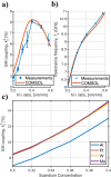
a, b A-posteriori 2D COMSOL® simulations of the devices shown in Fig. 3 and agreement with the experimental data in predicting kt2 a and fs b. The error bars show the maximum and minimum measured value per data point. In c, COMSOL® simulations of kt2 as function of Sc-doping of the piezoelectric film for different metal electrodes are provided. The simulated device has an h/λ ratio of 0.4. The IDT thicknesses are 95, 30, 40, and 70 nm for Al, Pt, W, and Mo, respectively. This optimal values were found via COMSOL® FEM.
Fig. 6
Fig. 6. Filter analysis.
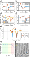
a, b Measured and de-embedded admittance responses of series and parallel resonators of F5 (Fig. 4a), c S21 of the de-embedded resonators and of the filter F5, and d comparison between measured and reconstructed filters from the responses shown in c. The discrepancy in the responses likely derives from the impact of pads and interconnects' parasitics. e) Measured S21 scattering parameters of a showcase filter as function of the input power. In f, the minimum IL degradation is plotted as function of the input power. The green region is the linear one, while the yellow indicates a input power region which causes a reversible IL degradation. The power levels in the red region cause irreversible device damage. In g, an SEM micrograph of the IDT fingers of the series resonator of the filter after experiencing 12 dBm of applied power. Electromigration is identified as IDTs breakdown mechanism.
Fig. 7
Fig. 7. On a further CLMR scaling.
Measured and BVD fitted admittance vs. frequency responses of resonators operating in the 14–20 GHz range, demonstrating the scaling capabilities of the LFE CLMR technology.

References

    1. Park, Y., Adachi, F., editors. Enhanced radio access technologies for next generation mobile communication. Dordrecht: Springer; (2007).
    1. History of mobile phones and the first mobile phone, https://www.uswitch.com/mobiles/guides/history-of-mobile-phones, accessed: 07.01.2022.
    1. 5G technology and networks (speed, use cases, rollout), https://www.thalesgroup.com/en/markets/digital-identity-and-security/mob..., accessed: 07.01.2022.
    1. Holma, Harry and Viswanathan, Harish and Mogenses, Preben Extreme massive MIMO for macro cell capacity boost in 5G-Advanced and 6G, White Paper, (2021).
    1. Yu, Y., Zhang, Y. & Zhu, J. Monolithic silicon micromachined Ka-band filters. In 2008 International Conference on Microwave and Millimeter Wave Technology (Vol. 3, pp. 1397–1400). IEEE (2008).