. 2024 Jan 9;15(1):387.
doi: 10.1038/s41467-023-44346-0.

Switchable tribology of ferroelectrics

Affiliations

Switchable tribology of ferroelectrics

Seongwoo Cho et al. Nat Commun. .

Abstract

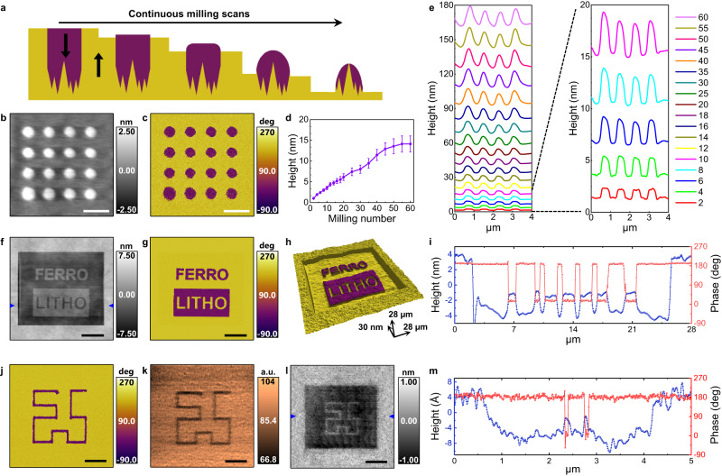
Switchable tribological properties of ferroelectrics offer an alternative route to visualize and control ferroelectric domains. Here, we observe the switchable friction and wear behavior of ferroelectrics using a nanoscale scanning probe-down domains have lower friction coefficients and show slower wear rates than up domains and can be used as smart masks. This asymmetry is enabled by flexoelectrically coupled polarization in the up and down domains under a sufficiently high contact force. Moreover, we determine that this polarization-sensitive tribological asymmetry is widely applicable across various ferroelectrics with different chemical compositions and crystalline symmetry. Finally, using this switchable tribology and multi-pass patterning with a domain-based dynamic smart mask, we demonstrate three-dimensional nanostructuring exploiting the asymmetric wear rates of up and down domains, which can, furthermore, be scaled up to technologically relevant (mm-cm) size. These findings demonstrate that ferroelectrics are electrically tunable tribological materials at the nanoscale for versatile applications.


Conflict of interest statement

The authors declare no competing interests.

Figures

Fig. 1
Fig. 1. Observation of asymmetric friction and wear of ferroelectric LiNbO3 single crystal.
a Schematic of asymmetric milling of periodically poled lithium niobate (PPLN) using a diamond probe. Ferroelectric up and down domains exhibit different mechanical wear rates after milling without any external voltage applied to the probe. Pristine up and down domains begin with identical initial topography but show different heights after repeated milling scans. b AFM height before milling, c friction image acquired during the 50th milling scan (scan angle of 90° with the fast scan axis perpendicular to domain walls). d, e AFM height (d) and PFM phase (e) after fifty milling scans show stable domain orientation after the wear process. Scale bars in (be) are 2 μm. f 3D surface plot of the patterned surface after 50 milling scans with a color scale indicating the PFM phase. The full-length scale along each respective axis is shown with an arrow. g Height and friction signal during the 50th milling scan. Arrows indicate the polarization orientation. h Height and friction difference between up and down domains with increasing scan number. After 10th, 20th and 30th milling scans (indicated by * and shaded color), intermediate PFM scans were conducted. i Schematic of large area milling by simply polishing the crystal using silica particles. jl Digital photograph of 3 × 3 mm2 PPLN (j), Optical microscope image (k) and scanning electron microscope image of patterned PPLN (l). m, n AFM height (m) and PFM phase (n) of large area milled PPLN. Scale bars are 3 mm for (j) 300 μm for (k) and 5 μm for (ln).
Fig. 2
Fig. 2. Origin of asymmetric friction and wear of ferroelectrics.
ac Schematic of flexoelectrically induced mechanism, in which the asymmetric tribological properties depend on the direction of the out-of-plane polarization, leading to a larger contact area during the scanning in up domains. The probe sinks deeper in the ferroelectric up domain than the down domain because of stiffness asymmetry (a). During the dynamic scan, the absolute value of the lateral signal in the position-sensitive photodiode is higher in the up domain than the down domain because of the larger contact area and indentation depth (b). The resulting height after continuous scans is higher in the down domain due to continuous milling with higher friction in the up domain (c). d Schematic of unscreened surface charge-driven mechanism. eg Computational mechanics approach of asymmetric friction in LiNbO3. Indentation depth (e) and contact area (f) of up and down domains based on cubic flexoelectricity with equal longitudinal and transversal coefficients corresponding to a flexocoupling coefficient of 10 V. Insets are magnifications of the red dotted area. Friction ratio (up/down) obtained from the numerical simulation and experiments (g). Flexocoupling coefficients simulated in (g) are between 1 and 10 V. Ten measurement points were averaged for each data point with error bars given by standard deviations. hj Investigation of tribological asymmetry with a non-conductive diamond probe. Friction during the milling scan with non-conductive probe (h), resulting AFM height (milled inside) with pristine background region (i) and PFM phase (j) using conductive diamond probe after one milling scan. kn Results of high voltage application to tip during the milling. Friction during the 1st milling scan (k) and line profiles in the 150 V, 0 V and −150 V regions (l). Arrows indicate the polarization orientation. Resulting AFM topography (m) and PFM phase (n) after 10 milling scans (scan angle of 90° with the fast scan axis perpendicular to the domain walls). Red circles indicate higher topography in electrically switched regions. Scale bars in (hn) are 5 μm.
Fig. 3
Fig. 3. Universal tribological asymmetry across a broad materials space.
The tribological asymmetry works universally regardless of the size and type of ferroelectric. ae Nanopillar fabrication on LiNbO3 single crystal by continuous mechanical milling after electrical switching, both with the same conductive diamond probe. Schematic of nanopillar fabrication (a). AFM height (b) and PFM phase (c) after ten milling scans at a loading force of 5 μN and a scan rate of 1.95 Hz. Scale bars in (b) and (c) are 1 μm. Average pillar height evolution with continuous milling scans (d). Pillar height was averaged from the line profiles across four pillars with 20 data points. The error bars indicate the standard deviations. Growth of nanopillars during continuous milling scans based on the line profiles from four pillars (e). Height data were acquired after the milling scan from 2 to 60 scans, as indicated by the color key. fh Ferroelectric nanostructure fabrication on thin LiNbO3 film. AFM height (f), PFM phase (g) and 3D surface images with color overlapped with their PFM phase (h). Scale bars in (f) and (g) are 6 μm. The full-length scale along each respective axis is shown with an arrow for (h). i Height and PFM phase line profiles along the blue marker in (f). jm Nanofabrication of PbTiO3 thin film. PFM phase after the artificial decoration of ferroelectric domains (j), Friction image during milling scans at 800 nN (k) and AFM height after multiple milling scans (l). Scale bars are 600 nm for (j) and (k) and 1 μm for (l). m Height and PFM phase line profile along the blue marker in (l).
Fig. 4
Fig. 4. 3D nanostructure fabrication using asymmetric nanotribology on ferroelectric LiNbO3 thin film.
a Schematic of top-down, chemical-free and maskless multi-patterning combining the switchable nature and asymmetric wear of ferroelectrics. b, c AFM height (b) and PFM phase (c) after multiple switching and patterning steps. d AFM height, including pristine background area, after multiple patterning. e Line profiles of height and PFM phase along the AFM probe feature in (b). f 3D representation of the multi-patterned structure with PFM phase color superimposed on the height image. Scale bars are 3 μm for (bd). The full-length scale along each respective axis is shown with an arrow for (f).

References

    1. Muralt P, Polcawich RG, Trolier-McKinstry S. Piezoelectric thin films for sensors, actuators, and energy harvesting. MRS Bull. 2009;34:658–664.
    1. Priya, S. & Inman, D. J. Energy Harvesting Technologies, Vol. 21 (Springer, 2009).
    1. Scott JF, Paz de Araujo CA. Ferroelectric memories. Science. 1989;246:1400–1405. - PubMed
    1. Jiang AQ, et al. Ferroelectric domain wall memory with embedded selector realized in LiNbO3 single crystals integrated on Si wafers. Nat. Mater. 2020;19:1188–1194. - PubMed
    1. Zubko, P., Catalan, G. & Tagantsev, A. K. Flexoelectric effect in solids. Ann. Rev. Mater. Res. 43, 387–421 (2013).