. 2024 Jan 20;15(1):630.
doi: 10.1038/s41467-024-44908-w.

Microwave quantum diode

Affiliations

Microwave quantum diode

Rishabh Upadhyay et al. Nat Commun. .

Abstract

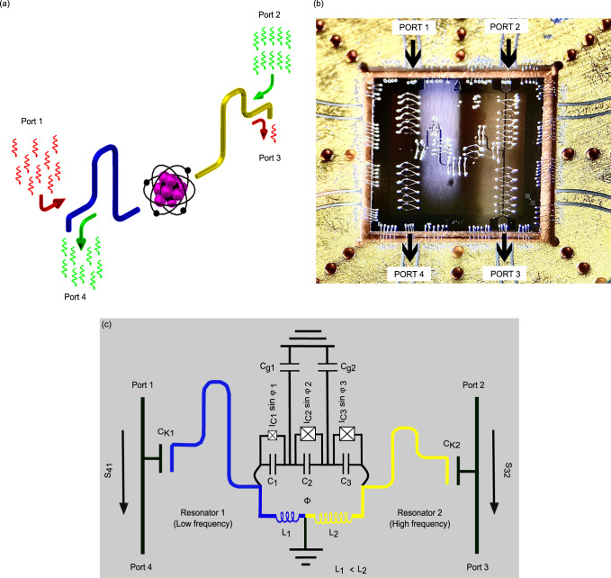
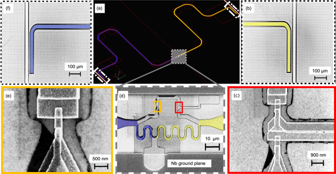
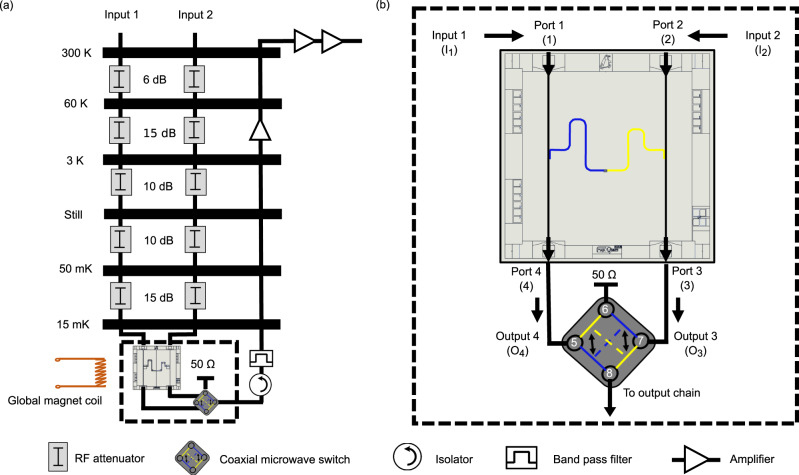
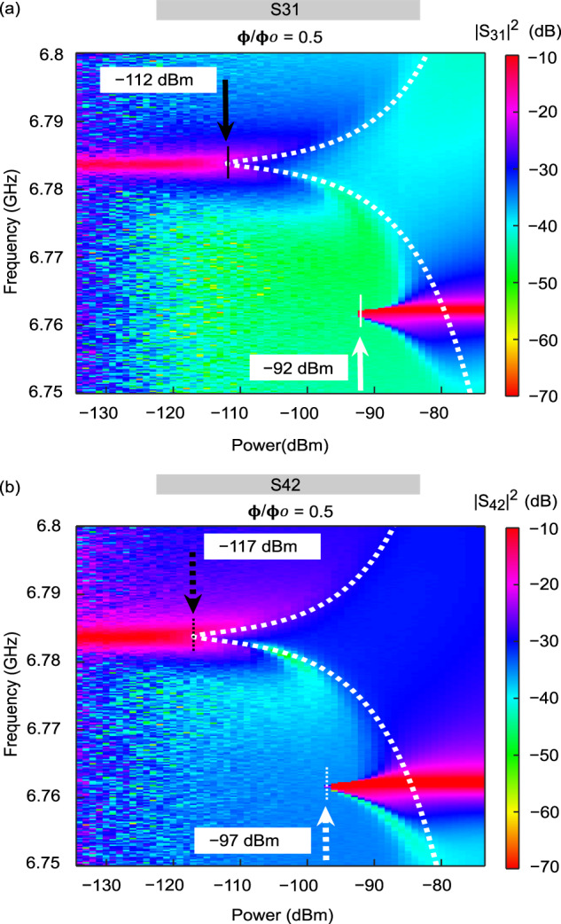
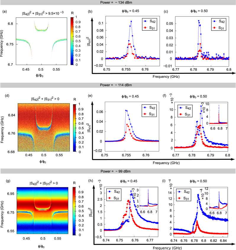
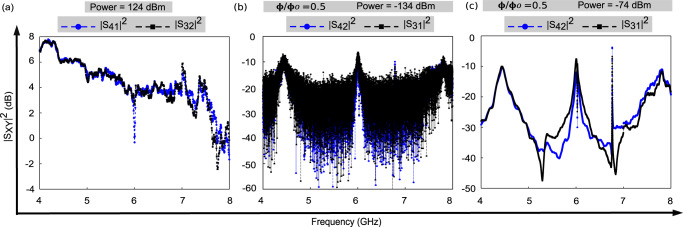
The fragile nature of quantum circuits is a major bottleneck to scalable quantum applications. Operating at cryogenic temperatures, quantum circuits are highly vulnerable to amplifier backaction and external noise. Non-reciprocal microwave devices such as circulators and isolators are used for this purpose. These devices have a considerable footprint in cryostats, limiting the scalability of quantum circuits. As a proof-of-concept, here we report a compact microwave diode architecture, which exploits the non-linearity of a superconducting flux qubit. At the qubit degeneracy point we experimentally demonstrate a significant difference between the power levels transmitted in opposite directions. The observations align with the proposed theoretical model. At - 99 dBm input power, and near the qubit-resonator avoided crossing region, we report the transmission rectification ratio exceeding 90% for a 50 MHz wide frequency range from 6.81 GHz to 6.86 GHz, and over 60% for the 250 MHz range from 6.67 GHz to 6.91 GHz. The presented architecture is compact, and easily scalable towards multiple readout channels, potentially opening up diverse opportunities in quantum information, microwave read-out and optomechanics.


Conflict of interest statement

The authors declare no competing interests.

Figures

Fig. 1
Fig. 1. The studied device.
a Conceptual representation of an artificial atom coupled to two resonators. The photons pass easily from the right side (green arrows, from port 2) to the left side (port 4), whereas those coming from left side (red arrow, from port 1) are mainly reflected back. b Optical microscope image of the device bonded on gold plated copper sample stage. The RF signal enters either via port 1 or port 2. Port 3 and Port 4 are the output ports. The black arrows indicate the direction of signal propagation. c Circuit model of the device. Here, Φ is the external magnetic flux threading through the qubit loop.
Fig. 2
Fig. 2. Electron micrographs of the reported device.
a The CAD layout of the device exhibiting the two resonators and the three-junction superconducting flux qubit at the center. The right and the left resonators are shown by yellow and by dark-blue colors respectively. The areas enclosed with white dotted lines at the top-right and bottom-left corner show the locations of the capacitors coupling the right and the left resonators with the feedlines. In (b, f) we show the magnified images of these capacitors. The gray shaded area close to the center in (a) shows a three-terminal flux qubit. Its zoomed image is shown in (d). The qubit is coupled to both resonators via the local inductances to the left and right, highlighted with different colors. c An enlarged electron micrograph of the two big junctions of the flux qubit. e Electron microscope image of the smaller qubit junction.
Fig. 3
Fig. 3. Measurement setup.
a Different temperature stages of the fridge with respective attenuation at each stage. The attenuation in the input lines 1 and 2 are nominally identical. b An enlarged image of the sample setup at the mixing chamber. Input 1 connects to the port 1 and input 2 --- to the port 2. The output ports 3 and 4 are connected to the coaxial microwave switch (Radiall R577 433002). The employed two-channel (channel A and channel B) switch is driven by a DC (V) bias. The factory defined RF continuity in the employed microwave switch for channel A is 5 → 8 and 7 → 6 (blue color in the switch cartoon), and for channel B is 5 → 6 and 7 → 8 (yellow color in the switch cartoon). It connects one of its input ports (output 4 in the figure) to the output read-out chain, and the same time it terminates the other input (output 3 in the figure) at 50 Ω impedance.
Fig. 4
Fig. 4. Measured transmission coefficient of the device as a function of the injected microwave power and frequency.
a Transmission coefficient ∣S312. b Transmission coefficient ∣S422. The color bars represent the transmission amplitude in dB. The dotted lines are the theoretically expected positions of the peak maxima given by Eq. (2). The observed maximum difference between the background transmission (without background calibration) is less than 10%, and can be considered as an error bar. See Background calibration under Section II for error analysis.
Fig. 5
Fig. 5. Data analysis for estimation of the transmission rectification ratio R.
a, d, g R of Eq. (1) measured at three different levels of the injected microwave power (P), −134 dBm, −114 dBm and −99 dBm. The color bar in (a, d, g) is the rectification ratio R. Here, Φ is the external magnetic flux and Φ0( = h/2e) is the magnetic flux quantum. At low input power −134 dBm, see panel a, the SNR is relatively poor. Here we extract the data points where the sum ∣S422 + ∣S312 exceeds certain threshold value. This threshold value is provided in the label above the graphs. In this way we avoid errors emerging from the background noise that could contribute to R at low input power. (b, e, h) Transmission coefficient ∣S312 and ∣S422 for the same three levels of power and at the flux value Φ/Φ0 = 0.45. c, f, i Transmission coefficient ∣S312 and ∣S422 at the flux value Φ/Φ0 = 0.5. The insets in (f, h, i are the plots with large x-axis from 6.52 to 7.02 GHz, of their main figures. The insertion loss and the isolation are reported in table I. Error bars for (ac) are ± 35%, whereas for (di) the error bars are below ± 10%. For more details on error estimation see error analysis under Section II.
Fig. 6
Fig. 6. Wide-band transmission coefficient graphs.
a Transmission coefficient plots for sides S41 and S32, reconstructed to obtain transmission baseline for background calibration. b, c Calibrated transmission coefficient plots obtained from Eqs. (7) and (8), measured across the device at −134 dBm and −74 dBm microwave power. The error bar is less than 10%, for more details see Background calibration under Section II.

References

    1. Clarke J, Wilhelm FK. Superconducting quantum bits. Nature. 2008;453:1031. doi: 10.1038/nature07128. - DOI - PubMed
    1. Wendin, G., & Shumeiko, V.S. Superconducting Quantum Circuits, Qubits and Computing. arXiv:cond-mat/0508729 (2005).
    1. Devoret, M.H., Wallraff, A. & Martinis, J.M. Superconducting Qubits: A Short Review. arXiv:cond-mat/0411174 (2004).
    1. Gu X, Kockum AF, Miranowicz A, Liu Y, Nori F. Microwave photonics with superconducting quantum circuits. Phys. Rep. 2017;718:1. doi: 10.1016/j.physrep.2017.10.002. - DOI
    1. Ronzani A, et al. Tunable photonic heat transport in a quantum heat valve. Nat. Phys. 2018;14:991. doi: 10.1038/s41567-018-0199-4. - DOI