. 2023 Mar 1;13(3):699-727.
doi: 10.1364/ome.484236. Epub 2023 Feb 22.

Recent Advances in Liquid Metal Photonics: Technologies and Applications

Affiliations

Recent Advances in Liquid Metal Photonics: Technologies and Applications

Peter Q Liu et al. Opt Mater Express. .

Abstract

Near-room-temperature liquid metals offer unique and crucial advantages over solid metals for a broad range of applications which require soft, stretchable and/or reconfigurable structures and devices. In particular, gallium-based liquid metals are the most suitable for a wide range of applications, not only owing to their low melting points, but also thanks to their low toxicity and negligible vapor pressure. In addition, gallium-based liquid metals exhibit attractive optical properties which make them highly suitable for a variety of photonics applications. This review summarizes the material properties of gallium-based liquid metals, highlights several effective techniques for fabricating liquid-metal-based structures and devices, and then focuses on the various photonics applications of these liquid metals in different spectral regions, following with a discussion on the challenges and opportunities for future research in this relatively nascent field.


Conflict of interest statement

Disclosures. The authors declare no conflicts of interest.

Figures

Fig. 1.
Fig. 1.
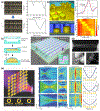
(a) Image of bulk liquid Ga pushed out of a syringe. (b) Image of a liquid EGaIn dipole antenna in a PDMS mold. Adapted with permission from [5]. Copyright the Royal Society of Chemistry 2015. (c) SEM image of liquid Ga NPs formed on a silicon substrate by MBE deposition.
Fig. 2.
Fig. 2.
(a) Relative permittivity functions of Ga in solid and liquid phases. Data obtained from [26]. (b) Imaginary part of relative permittivity from randomly distributed liquid Ga NPs on sapphire substrates. Adapted with permission from [29]. Copyright American Institute of Physics 2007. (c) Hyperspectral cathodoluminescence images of individual Ga NPs at 380, 430, 500, and 800 nm. Adapted with permission from [26]. Copyright American Chemical Society 2015.
Fig. 3.
Fig. 3.
(a) Schematics of the procedure for forming liquid metal structures in a elastomer mold. Adapted with permission from [35]. Copyright Wiley 2014. (b) Schematics of the procedure for forming liquid metal structures based on selective wetting. Adapted with permission from [39]. Copyright Elsevier 2015. (c) Schematic of fabricating liquid metal structures by direct writing. Adapted with permission from [42]. Copyright Wiley2014. (d) Image of a 3D printed liquid metal structure. The scale bar represents 500 μm. Adapted with permission from [45]. Copyright Wiley 2013.
Fig. 4.
Fig. 4.
(a) Optical image and schematic of a microfluidic flow focusing device for producing liquid EGaIn microparticles. Adapted with permission from [49]. Copyright Royal Society of Chemistry 2012. (b) Schematic of a microfluidic flow focusing device combined with ultrasonic wave agitation for producing liquid EGaIn NPs. Adapted with permission from [51]. Copyright Wiley 2018. (c) Schematic illustration of the SLICE process for transforming bulk liquid metal into microparticles and NPs. Adapted with permission from [52]. Copyright Americal Chemical Society 2014. (d) Schematic illustration of the ultrasonication process for transforming bulk liquid metal into NPs. Adapted with permission from [54]. Copyright Wiley 2016. (e) Schematic illustration and SEM images of Ga NPs formed on a silicon substrate by MBE deposition. Adapted with permission from [26]. Copyright American Chemical Society 2015. (f) Schematic illustration of the synthesis of Ga NPs via galvanic replacement reaction of sacrificial Zn NPs. Adapted with permission from [61].Copyright Royal Society of Chemistry 2021.
Fig. 5.
Fig. 5.
(a) Schematics and simulated field distributions of the in-plane (longitudinal) and out-of-plane (transverse) SPR modes of liquid Ga NPs on a substrate. Adapted with permission from [26]. Copyright American Chemical Society 2015. (b) Schematics of the fabrication process of Ga gratings and the reflection spectrum change of the Ga gratings induced by the Ga solid-liquid phase transition. Adapted with permission from [66]. Copyright Americal Chemical Society 2012. (c) SEM images from a 30°-tilted view of Ga NPs after anodization for different durations and after thermal oxidation at 300 °C for 5 min. Adapted with permission from [65]. Copyright Chen et al. 2022. (d) SEM images of the Al nanostructured templates of different pit diameters (first column), Ga NPs on Al templates (second column) and on flat Si (third). Adapted with permission from [71]. Copyright Catalán-Gómez et al. 2020. (e) Left: schematic representing the flux and temperature conditions to obtain core–shell, alloy, or phase-segregated GaMg NPs. Middle: Real-time evolution of the imaginary part of the pseudodielectric dielectric function during GaMg NP deposition. Right: Dependence of SPR energy of GaMg alloy NPs of various compositions with a diameter of approximately 55 nm. Adapted with permission from [74]. Copyright Wiley 2011.
Fig. 6.
Fig. 6.
(a) Top: size distribution and SEM image of a SERS substrate with liquid Ga NPs. Bottom: Raman spectra obtained from three SERS substrates with different liquid Ga NP size distributions. The inset shows the LSPR characteristics of the three SERS substrates. Adapted with permission from [78]. Copyright Americal Chemical Society 2013. (b) Schematic illustrations of the liquid Ga NP-based DNA biosensor. Adapted with permission from [82]. Copyright Royal Society of Chemistry 2016. (c) Left: SEM image of liquid Ga NPs on MoS2 flakes on a sapphire substrate. Right: Photoluminescence spectra from MoS2 flakes with and without liquid Ga NPs. Adapted with permission from [83]. Copyright Royal Society of Chemistry 2019. (d) Upper left: schematic of a hemispherical liquid Ga NP functioning as a plasmonic antenna and a photocatalytic nanoreactor for hydrogen dissociation, storage, and hydrogen spillover as well as oxygen-reverse spillover. Upper right: Near-field enhancement profile of the hemispherical liquid Ga NP. Lower: SEM and TEM images of the Ga/Al2O3 interface showing the formation of Ga2O3 localized at the interface upon hydrogen interaction. Adapted with permission from [84]. Copyright Wiley 2021.
Fig. 7.
Fig. 7.
(a) Transient light-induced reflectivity increase in Ga films on Si measured with 150-fs 800-nm pump and probe pulses at various pump energy densities. Adapted with permission from [86]. Copyright Optical Society of America 2001. (b) Top: schematic of the passively Q-switched fiber laser cavities, consisting of a liquefying Ga mirror as the nonlinear element. Bottom: Output power characteristic of the erbium fiber laser with a liquefying Ga mirror, showing the region of stable Q-switching, and a typical output pulse obtained at a pump power of 1.09 W (inset). Adapted with permission from [88]. Copyright American Institute of Physics 1999. (c) Unit cell design of a Ga-backplane/Si3N4/gold-disc metasurface absorber with a resonant wavelength of 1310 nm. (d) Top: absolute 1550 nm reflectivity of the metasurface in (c) as a function of time during and after excitation with a 500 μs, 9.5 μW/μm2 pump pulse at 1310 nm, for various sample temperatures. Bottom: maximum induced 1550 nm reflectivity change for various 1310 nm pump intensities as a function of sample temperature. The inset shows reflectivity relaxation time as a function of temperature and pump intensity. (c)&(d) adapted with permission from [92]. Copyright American Institute of Physics 2015. (e) Simplified generic diagram illustrating quaternary memory functionality in a Ga NP, employing four different phases, each labeled as a unique logical state. (f) Quaternary memory functionality of the Ga NP, with the particle state monitored using the pump-probe technique. (e)&(f) adapted with permission from [95]. Copyright American Physical Society 2007.
Fig. 8.
Fig. 8.
(a) Schematic illustration of the liquid-Ga-based nanopatch antenna SEIRA sensor. (b) Simulated field enhancement profile of the liquid Ga-based nanopatch antenna SEIRA sensor. (c) Left: measured reflection spectra of liquid-Ga-based SEIRA sensors with monolayer ODT showing the ODT vibrational modes. Right: Extracted net SEIRA signals associated with the monolayer ODT. (a)-(c) adapted with permission from [99]. Copyright Wiley 2022. (d) Top: SEM images of 400 nm Ga evaporated onto treated PDMS under high vacuum and low vacuum, respectively. Bottom: SEM images showing a liquid Ga metasurface structure at 0% and 50% strain of the PDMS substrate, respectively. (e) Experimental (left) and simulated (right) reflection spectra for 2 μm period square metasurfaces with 1.5 μm liquid Ga disks at various strains using light polarized perpendicular to the tensile axis. (d)&(e) adapted with permission from [100]. Copyright Wiley 2020.
Fig. 9.
Fig. 9.
(a) Top: image of a portion of the split ring resonator array and its transmission spectrum. Bottom: image of a portion of the closed ring resonator array and its transmission spectrum. The closed ring resonators are transformed from the split ring resonators by applying higher pressure to inject liquid metal into the narrower channel section. Adapted with permission from [104]. Copyright Optical Society of America 2014. (b) Left: Schematic of the liquid-metal-based metasurface consisting of the liquid-metal-pillar array embedded in silicon cavities. Upper right: Absorption spectra with TE mode (red line) and TM mode (blue dot) when the height of liquid-metal-pillars is 70 μm. Lower right: Absorption color map for the TM mode when the height of the liquid-metal-pillars is tuned from 30 μm to 90 μm. Adapted with permission from [105]. Copyright Song et al. 2017. (c) Schematic illustrations of a deformable liquid-metal-based THz metasurface and the mechanism for inducing deformation and hence spectral response change. Reprinted with permission from [106]. Copyright Optical Society of America 2021. (d) Images of a liquid-metal antenna being stretched, rolled and cut. The antenna self-heals in response to sharp cuts. Adapted with permission from [108]. Copyright Wiley 2009. (e) Left: Schematic illustration of a randomly addressable metasurface as a flat lens with tunable focal distance when resonant properties of the split rings in the array are altered by changing the metal filling fraction. Right: Simulation and experimental results showing the tuning of the metasurface lens’ focus when the spatial phase distribution (the fourth column) is changed. Adapted with permission from [116]. Copyright Wiley 2015.

Similar articles

Cited by

References

    1. Linic S, Christopher P, and Ingram DB, “Plasmonic-metal nanostructures for efficient conversion of solar to chemical energy,” Nature Materials 10, 911 (2011). - PubMed
    1. Boltasseva A, and Atwater H, “Low-loss plasmonic metamaterials,” Science 331, 290 (2011). - PubMed
    1. Handschuh-Wang S, Stadler FJ, and Zhou X, “Critical review on the physical properties of gallium-based liquid metals and selected pathways for their alteration,” Journal of Physical Chemistry C 125, 20113 (2021).
    1. Chitambar CR, “Medical applications and toxicities of gallium compounds,” International Journal of Environmental Research and Public Health 7, 2337–2361 (2010). - PMC - PubMed
    1. Joshipura ID, Ayers HR, Majidi C, and Dickey MD, “Methods to pattern liquid metals,” Journal of Materials Chemistry C 3, 3834 (2015).

LinkOut - more resources