Review on Main Gate Characteristics of P-Type GaN Gate High-Electron-Mobility Transistors
- PMID: 38258199
- PMCID: PMC10818513
- DOI: 10.3390/mi15010080
Review on Main Gate Characteristics of P-Type GaN Gate High-Electron-Mobility Transistors
Abstract
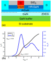
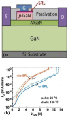
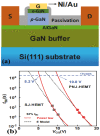
As wide bandgap semiconductors, gallium nitride (GaN) lateral high-electron-mobility transistors (HEMTs) possess high breakdown voltage, low resistance and high frequency performance. PGaN gate HEMTs are promising candidates for high-voltage, high-power applications due to the normally off operation and robust gate reliability. However, the threshold and gate-breakdown voltages are relatively low compared with Si-based and SiC-based power MOSFETs. The epitaxial layers and device structures were optimized to enhance the main characteristics of pGaN HEMTs. In this work, various methods to improve threshold and gate-breakdown voltages are presented, such as the top-layer optimization of the pGaN cap, hole-concentration enhancement, the low-work-function gate electrode, and the MIS-type pGaN gate. The discussion of the main gate characteristic enhancement of p-type GaN gate HEMTs would accelerate the development of GaN power electronics to some extent.
Keywords: breakdown field; gallium nitride; gate-breakdown voltage; p-type doped gallium nitride high-electron-mobility transistor (p-GaN HEMT); threshold voltage.
Conflict of interest statement
The authors declare no conflict of interest.
Figures


Similar articles
-
GaN-based complementary inverter logic gate using InGaN/GaN superlattice capped enhancement-mode field-effect-transistors.Nanotechnology. 2021 May 12;32(31). doi: 10.1088/1361-6528/abfb99. Nanotechnology. 2021. PMID: 33902018
-
Analysis of Operational Characteristics of AlGaN/GaN High-Electron-Mobility Transistor with Various Slant-Gate-Based Structures: A Simulation Study.Micromachines (Basel). 2022 Nov 11;13(11):1957. doi: 10.3390/mi13111957. Micromachines (Basel). 2022. PMID: 36422387 Free PMC article.
-
High Thermal Dissipation of Normally off p-GaN Gate AlGaN/GaN HEMTs on 6-Inch N-Doped Low-Resistivity SiC Substrate.Micromachines (Basel). 2021 May 1;12(5):509. doi: 10.3390/mi12050509. Micromachines (Basel). 2021. PMID: 34062908 Free PMC article.
-
An Overview of Normally-Off GaN-Based High Electron Mobility Transistors.Materials (Basel). 2019 May 15;12(10):1599. doi: 10.3390/ma12101599. Materials (Basel). 2019. PMID: 31096689 Free PMC article. Review.
-
Status of Aluminum Oxide Gate Dielectric Technology for Insulated-Gate GaN-Based Devices.Materials (Basel). 2022 Jan 21;15(3):791. doi: 10.3390/ma15030791. Materials (Basel). 2022. PMID: 35160737 Free PMC article. Review.
References
-
- Tsou C.W., Kang H.C., Lian Y.W., Shawn S.H. AlGaN/GaN HEMTs on silicon with hybrid Schottky-ohmic drain for RF applications. IEEE Trans. Electron Devices. 2016;23:4218–4221. doi: 10.1109/TED.2016.2605128. - DOI
-
- Wang F., Chen W., Li X., Sun R., Xu X., Xin Y., Wang Z., Shi Y., Xia Y., Liu C. Charge storage impact on input capacitance in p-GaN gate AlGaN/GaN power high-electron-mobility transistors. J. Phys. D Appl. Phys. 2020;53:305106. doi: 10.1088/1361-6463/ab86e7. - DOI
-
- Wang F., Chen W., Xu X., Sun R., Wang Z., Xia Y., Xin Y., Zhou Q., Zhang B. Simulation study of an ultralow switching loss p-GaN gate HEMT with dynamic charge storage mechanism. IEEE Trans. Electron Devices. 2021;68:175–183. doi: 10.1109/TED.2020.3036325. - DOI
-
- Chen K.J., Häberlen O., Lidow A., Lin C., Ueda T., Uemoto Y., Wu Y. GaN-on-Si power technology: Devices and applications. IEEE Trans. Electron Devices. 2017;64:779–795. doi: 10.1109/TED.2017.2657579. - DOI
-
- Kwon W., Kawasaki S., Watanabe H., Tanaka A., Honda Y., Ikeda H., Iso K., Amano H. Reverse leakage mechanism of dislocation-free GaN vertical p-n diodes. IEEE Electron Device Lett. 2023;44:1172–1175. doi: 10.1109/LED.2023.3274306. - DOI
Publication types
LinkOut - more resources
Full Text Sources
Research Materials
Miscellaneous

