

Laser-driven noncontact bubble transfer printing via a hydrogel composite stamp
- PMID: 38266054
- PMCID: PMC10835071
- DOI: 10.1073/pnas.2318739121
Laser-driven noncontact bubble transfer printing via a hydrogel composite stamp
Abstract
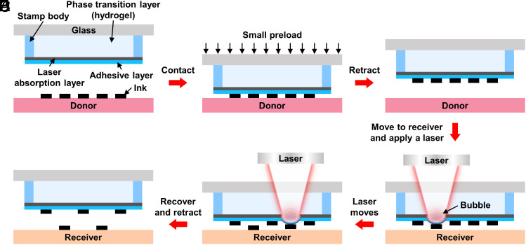
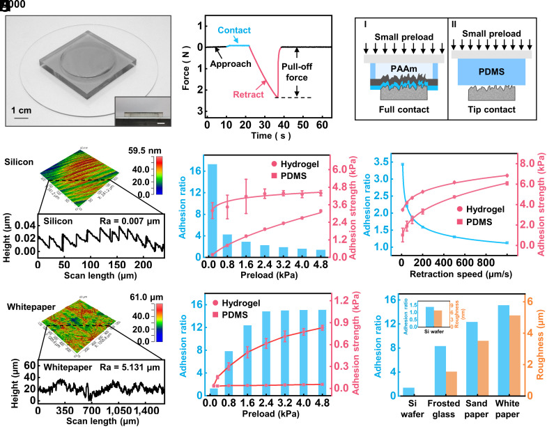
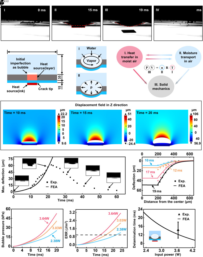
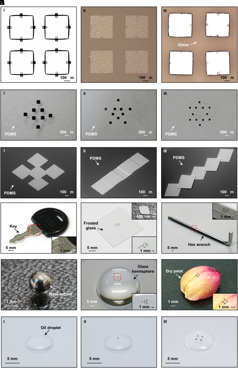
Transfer printing that enables heterogeneous integration of materials into spatially organized, functional arrangements is essential for developing unconventional electronic systems. Here, we report a laser-driven noncontact bubble transfer printing via a hydrogel composite stamp, which features a circular reservoir filled with hydrogel inside a stamp body and encapsulated by a laser absorption layer and an adhesion layer. This composite structure of stamp provides a reversible thermal controlled adhesion in a rapid manner through the liquid-gas phase transition of water in the hydrogel. The ultrasoft nature of hydrogel minimizes the influence of preload on the pick-up performance, which offers a strong interfacial adhesion under a small preload for a reliable damage-free pick-up. The strong light-matter interaction at the interface induces a liquid-gas phase transition to form a bulge on the stamp surface, which eliminates the interfacial adhesion for a successful noncontact printing. Demonstrations of noncontact transfer printing of microscale Si platelets onto various challenging nonadhesive surfaces (e.g., glass, key, wrench, steel sphere, dry petal, droplet) in two-dimensional or three-dimensional layouts illustrate the unusual capabilities for deterministic assembly to develop unconventional electronic systems such as flexible inorganic electronics, curved electronics, and micro-LED display.
Keywords: adhesion strength; hydrogel stamp; laser-driven; transfer printing.
Conflict of interest statement
Competing interests statement:The authors declare no competing interest.
Figures
Similar articles
-
Switchable Adhesive Based on Shape Memory Polymer with Micropillars of Different Heights for Laser-Driven Noncontact Transfer Printing.ACS Appl Mater Interfaces. 2024 Feb 21;16(7):9443-9452. doi: 10.1021/acsami.3c16282. Epub 2024 Feb 9. ACS Appl Mater Interfaces. 2024. PMID: 38335021
-
Laser-driven programmable non-contact transfer printing of objects onto arbitrary receivers via an active elastomeric microstructured stamp.Natl Sci Rev. 2020 Feb;7(2):296-304. doi: 10.1093/nsr/nwz109. Epub 2019 Aug 6. Natl Sci Rev. 2020. PMID: 34692045 Free PMC article.
-
Programmable and scalable transfer printing with high reliability and efficiency for flexible inorganic electronics.Sci Adv. 2020 Jun 17;6(25):eabb2393. doi: 10.1126/sciadv.abb2393. eCollection 2020 Jun. Sci Adv. 2020. PMID: 32596472 Free PMC article.
-
Transfer Printing of Electronic Functions on Arbitrary Complex Surfaces.ACS Nano. 2020 Jan 28;14(1):12-20. doi: 10.1021/acsnano.9b09846. Epub 2020 Jan 8. ACS Nano. 2020. PMID: 31913600 Review.
-
Transfer printing techniques for materials assembly and micro/nanodevice fabrication.Adv Mater. 2012 Oct 9;24(39):5284-318. doi: 10.1002/adma.201201386. Epub 2012 Aug 31. Adv Mater. 2012. PMID: 22936418 Review.
Cited by
-
Laser-induced adhesives with excellent adhesion enhancement and reduction capabilities for transfer printing of microchips.Sci Adv. 2024 Dec 6;10(49):eads9226. doi: 10.1126/sciadv.ads9226. Epub 2024 Dec 6. Sci Adv. 2024. PMID: 39642216 Free PMC article.
-
Gecko Toe Pad-Inspired Robotic Gripper with Rapidly and Precisely Tunable Adhesion.Research (Wash D C). 2025 Apr 23;8:0687. doi: 10.34133/research.0687. eCollection 2025. Research (Wash D C). 2025. PMID: 40270692 Free PMC article.
-
Wafer-Scale Replication of Plasmonic Nanostructures via Microbubbles for Nanophotonics.Adv Sci (Weinh). 2024 Oct;11(40):e2404870. doi: 10.1002/advs.202404870. Epub 2024 Sep 3. Adv Sci (Weinh). 2024. PMID: 39225406 Free PMC article.
-
Shape memory polymer surfaces with controllable roughness for multiscale switchable dry adhesion.Nat Commun. 2025 May 28;16(1):4954. doi: 10.1038/s41467-025-60220-7. Nat Commun. 2025. PMID: 40436828 Free PMC article.
-
Flexible Mechanical Sensors for Plant Growth Monitoring: An Emerging Area for Smart Agriculture.Sensors (Basel). 2024 Dec 14;24(24):7995. doi: 10.3390/s24247995. Sensors (Basel). 2024. PMID: 39771731 Free PMC article.
References
-
- Zhang W., Zhang L., Liao Y., Cheng H., Conformal manufacturing of soft deformable sensors on the curved surface. Int. J. Extrem. Manuf. 3, 042001 (2021).
-
- Rich S. I., Jiang Z., Fukuda K., Someya T., Well-rounded devices: The fabrication of electronics on curved surfaces–A review. Mater. Horiz. 8, 1926–1958 (2021). - PubMed
-
- Wu H., et al. , Fabrication techniques for curved electronics on arbitrary surfaces. Adv. Mater. Technol. 5, 2000093 (2020).
-
- Chen Z., Yan S. K., Danesh C., Microled technologies and applications: Characteristics, fabrication, progress, and challenges. J. Phys. D: Appl. Phys. 54, 34 (2021).
Grants and funding
- U21A20502/MOST | National Natural Science Foundation of China (NSFC)
- 12225209/MOST | National Natural Science Foundation of China (NSFC)
- U20A6001/MOST | National Natural Science Foundation of China (NSFC)
- 12321002/MOST | National Natural Science Foundation of China (NSFC)
- 2022YFC2401901/MOST | National Key Research and Development Program of China (NKPs)
LinkOut - more resources
Full Text Sources
