. 2024 Jan 24;15(1):694.
doi: 10.1038/s41467-024-44790-6.

EUV-induced hydrogen desorption as a step towards large-scale silicon quantum device patterning

Affiliations

EUV-induced hydrogen desorption as a step towards large-scale silicon quantum device patterning

Procopios Constantinou et al. Nat Commun. .

Abstract

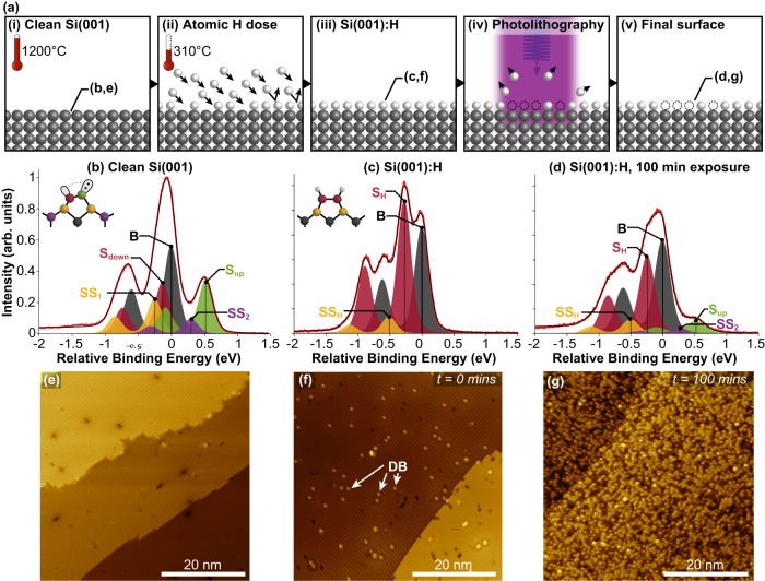
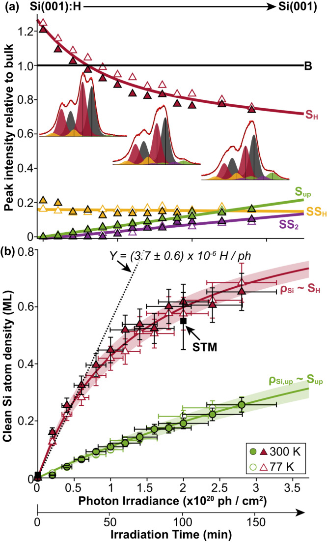
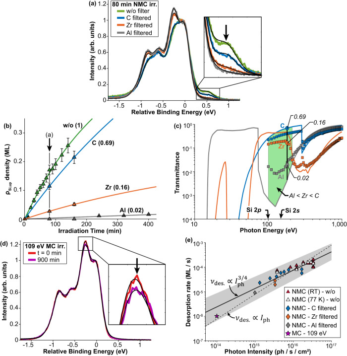
Atomically precise hydrogen desorption lithography using scanning tunnelling microscopy (STM) has enabled the development of single-atom, quantum-electronic devices on a laboratory scale. Scaling up this technology to mass-produce these devices requires bridging the gap between the precision of STM and the processes used in next-generation semiconductor manufacturing. Here, we demonstrate the ability to remove hydrogen from a monohydride Si(001):H surface using extreme ultraviolet (EUV) light. We quantify the desorption characteristics using various techniques, including STM, X-ray photoelectron spectroscopy (XPS), and photoemission electron microscopy (XPEEM). Our results show that desorption is induced by secondary electrons from valence band excitations, consistent with an exactly solvable non-linear differential equation and compatible with the current 13.5 nm (~92 eV) EUV standard for photolithography; the data imply useful exposure times of order minutes for the 300 W sources characteristic of EUV infrastructure. This is an important step towards the EUV patterning of silicon surfaces without traditional resists, by offering the possibility for parallel processing in the fabrication of classical and quantum devices through deterministic doping.


Conflict of interest statement

The authors declare no competing interests.

Figures

Fig. 1
Fig. 1. Photon-based hydrogen desorption lithography characterised with combined XPS and STM.
a Process flow of photon-based hydrogen desorption lithography. In steps (i), (iii) and (v), in situ XPS and STM experiments were performed, whose data are presented in (b, e), (c, f) and (d, g), respectively. b Photoelectron spectrum of the clean Si(001) surface. The five fitted components Sup, Sdown, SS1, SS2 (520, −150, −240 and 240 meV) and B are all individually identified, and colour-coded to the surface reconstruction shown to the left. The uppermost dimers are buckled due to the charge transfer of the π-orbital. c Photoelectron spectrum of the hydrogen terminated Si(001):H surface. The three fitted components SH, SSH and B are all individually identified (with an energy shift of −250 and −450 meV, respectively) and colour-coded to the surface reconstruction to the left. d Photoelectron spectrum of the Si(001):H surface after 100 min of non-monochromatic irradiation, revealing the emergence of dangling bonds (DBs). All XPS data are for a photon energy  = 140 eV at θ = 60° and the binding energies are measured relative to the bulk component, B. The solid red and black lines show the raw and fitted data, respectively, prior to background subtraction, whose maximum peak height is scaled to one. Each fit component is plotted after background subtraction and each energy shift has an uncertainty of 50 meV. eg Corresponding STM data (−2.5 V, 50 pA) taken on the same region as the XPS for each surface.
Fig. 2
Fig. 2. Estimated clean silicon atom density versus non-monochromatic photon irradiance.
a Plot of the intensities of the Si 2p peak components (labelled and colour-coded) versus the non-monochromatic irradiation time/irradiance (see Methods for the definition of the photon irradiance). The bulk (B) peak intensity is normalised to one and the solid lines are guides to the eye. The inset XPS data at 20, 80 and 120 min illustrate the change of the Si 2p spectrum with hydrogen desorption. The XPS fits at each 20 min interval are shown in Supplementary Fig. 2. b Density of clean silicon atoms, ρSi (red triangles) and up-buckled silicon atoms, ρSi,up (green circles) versus non-monochromatic irradiation time/irradiance. The black data point at 100 min irradiation time shows the silicon atom density, as measured from the STM image. Data were taken at both room temperature (filled symbols) and 77 K (empty symbols), where the temperature was kept the same during both the desorption and measuring steps. The coloured areas around the fits represent the 90% confidence interval. In the linear regime, the desorption yield, Y, is equal to the gradient of the dotted black line. The experimental data and fits (solid lines) are performed over the domain 0 – 2.75 × 1020 ph/cm2 (or 0 – 140 min) using a one-parameter fit in accordance with Eq. 3. For ρSi, the best fit yields σ = (0.7 ± 0.1) × 10−20 cm2 and νdes. = (0.015 ± 0.001) ML/min for the photon irradiance and irradiation time domain, respectively. The vertical error bars of the STM were determined from repeated measurements at different locations on the surface, whereas the error bars from the XPS data was ~10%, derived from the curve fits. The horizontal error bars for the time domain are ~ 1 min, however, this is higher when transformed into photon irradiance due to the uncertainty of the photon flux and spot-size.
Fig. 3
Fig. 3. Extreme ultraviolet (EUV) photon energy bandwidth for hydrogen desorption.
a Si 2p photoelectron spectrum taken after 80 min photon irradiation using non-monochromatic (NMC) light without (w/o) and with three different EUV filters from a Si(001):H surface. A zoom-in of the single dangling bond component is shown by the arrow. b Plot of the density of up-buckled silicon atoms, ρSi,up, as a function of photon irradiation time (symbols), along with their best fits (lines). Each filter is labelled along with its comparative desorption rate relative to its unfiltered value. c Plot of the calculated (solid lines) and experimental (symbols) transmission curves for each EUV filter. The green region spans the photon energy range 100–210 eV where the transmission profile is such that Al < Zr < C; this coincides with the observed desorption rates in (a, b) and represents the photon energy regime responsible for the hydrogen desorption. The arrows indicate the threshold energy of the Si 2p and Si 2s core-levels, which lie within the green region. d Si 2p photoelectron spectrum taken after 900 min photon irradiation using monochromatic (MC) light at 109 eV. A zoom-in of the hydrogenic component is shown; the arrow indicates a very small decrease, due to hydrogen desorption. e Log-log plot of the desorption rate, νdes., as a function of incident photon intensity, Iph. The shaded area around the fit represents the 90% confidence interval. The NMC exposures are shown for both 77 K and RT, whereas the filtered NMC and MC exposures are at RT. The solid and dashed lines show the best fit for an exponent that equals 3/4 (sub-linear) and 1 (linear), respectively.
Fig. 4
Fig. 4. Demonstrating hydrogen desorption in the EUV range using XPEEM at the SIM beamline.
a, c XPEEM images taken with a start voltage of −0.8 V and 50 μm field-of-view after a (a) 93 eV and (c) 106 eV irradiation for 157 min. A vertical, rectangular band was irradiated by narrowing the beamline exit slit to be smaller than the PEEM field-of-view, after which it was widened to reveal both the unexposed and irradiated areas (see Methods for more details). b, d A cumulative series of secondary electron (SE) curves, extracted every 1 min during the (b) 93 eV and (d) 106 eV irradiations. In (b), a shift of the SE peak of +0.3 V is observed. In (d) the vertical, black, solid lines indicate the SE peak position (at 0 min) and the Si 2p photoelectron peak position. In (c), the inset at the bottom shows a line profile extracted from the XPEEM image (denoted by the yellow, dashed line), with the measured FWHM of the edge being 4.5 μm. e Plot of the density of clean silicon atoms as a function of the photon irradiance. The purple and green curves show the results from the SIM beamline irradiation and the red curve is the best fit made to the PEARL experiments of Fig. 2b. Note that the presence of the Si 2p shoulder in (d) can obfuscate the true SE peak height, causing it to be underestimated; this is what causes the purple curve in (e) to deviate from the PEARL curve. This is absent in (b), where only a single SE peak is observed, since 93 eV is below the Si 2p excitation threshold. In (e), the vertical error-bars are ~0.02 ML.
Fig. 5
Fig. 5. Illustration of a proposed laboratory process flow of patterning silicon quantum devices, divided into four stages.
In the upper-right panel, we show the proposed UHV setup that can be integrated at the EUV-IL system at the XIL beamline of the SLS. The load-lock (LL) is where the silicon substrates are introduced into vacuum and then transferred to the transfer chamber. Three chambers are branched from the transfer chamber, all of which have a UHV environment with a base pressure < 5 × 10−10 mbar: the preparation, EUV-lithography and STM chamber. The preparation chamber is used for annealing, hydrogen passivation, XH3 dosing and silicon MBE growth. The EUV-Lithography chamber is used for the EUV hydrogen desorption lithography. The STM chamber is used to gauge the quality of the surface at each stage and to perform atomic-scale hydrogen-desorption lithography. There are 4 main stages when it comes to fabricating silicon quantum devices; Stage 1: The process begins with preparing a clean silicon surface, followed by the atomic hydrogen passivation of Si(001). Stage 2: EUV hydrogen-desorption lithography of large-scale contacts. Stage 3: STM or EUV hydrogen-desorption lithography for patterning the nm-scale quantum device at the centre of the fiduciary markers. Stage 4: Dopant incorporation and silicon encapsulation. After this, the sample can be extracted from UHV into ambient and standard cleanroom processing techniques can be used to contact the buried device with vertical electrical connections.

References

    1. Schofield SR, et al. Atomically precise placement of single dopants in Si. Phys. Rev. Lett. 2003;91:136104. doi: 10.1103/PhysRevLett.91.136104. - DOI - PubMed
    1. Stock TJZ, et al. Atomic-scale patterning of arsenic in silicon by scanning tunneling microscopy. ACS Nano. 2020;14:3316–3327. doi: 10.1021/acsnano.9b08943. - DOI - PMC - PubMed
    1. Škereň T, Köster SA, Douhard B, Fleischmann C, Fuhrer A. Bipolar device fabrication using a scanning tunnelling microscope. Nat. Electron. 2020;3:524–530. doi: 10.1038/s41928-020-0445-5. - DOI
    1. Campbell, Q. et al. Reaction pathways of BCl3 for acceptor delta-doping of silicon. 2022 [Online]. Available: http://arxiv.org/abs/2201.11682.
    1. Kane BE. A silicon-based nuclear spin quantum computer. Nature. 1998;393:133–137. doi: 10.1038/30156. - DOI