

Influence of annealing pretreatment in different atmospheres on crystallization quality and UV photosensitivity of gallium oxide films
- PMID: 38312726
- PMCID: PMC10836329
- DOI: 10.1039/d3ra07568k
Influence of annealing pretreatment in different atmospheres on crystallization quality and UV photosensitivity of gallium oxide films
Abstract
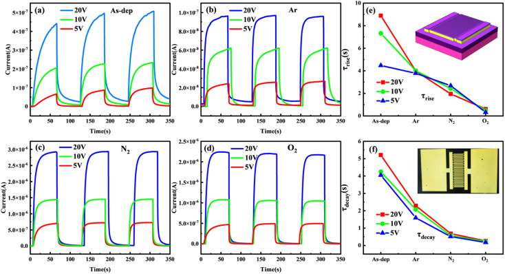
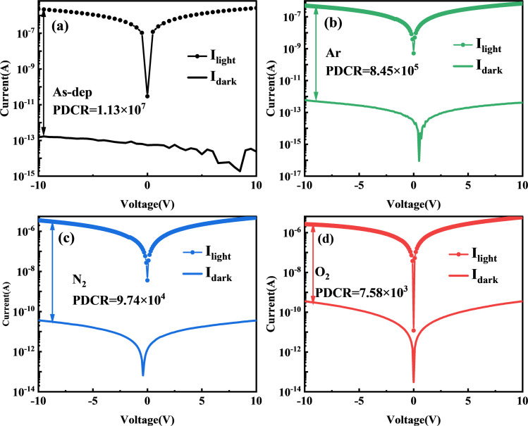
Due to their high wavelength selectivity and strong anti-interference capability, solar-blind UV photodetectors hold broad and important application prospects in fields like flame detection, missile warnings, and secure communication. Research on solar-blind UV detectors for amorphous Ga2O3 is still in its early stages. The presence of intrinsic defects related to oxygen vacancies significantly affects the photodetection performance of amorphous Ga2O3 materials. This paper focuses on growing high quality amorphous Ga2O3 films on silicon substrates through atomic layer deposition. The study investigates the impact of annealing atmospheres on Ga2O3 films and designs a blind UV detector for Ga2O3. Characterization techniques including atomic force microscopy (AFM), X-ray diffraction (XRD) and X-ray photoelectron spectroscopy (XPS) are used for Ga2O3 film analysis. Ga2O3 films exhibit a clear transition from amorphous to polycrystalline after annealing, accompanied by a decrease in oxygen vacancy concentration from 21.26% to 6.54%. As a result, the response time of the annealed detector reduces from 9.32 s to 0.47 s at an external bias of 10 V. This work demonstrates that an appropriate annealing process can yield high-quality Ga2O3 films, and holds potential for advancing high-performance solar blind photodetector (SBPD) development.
This journal is © The Royal Society of Chemistry.
Conflict of interest statement
The authors declare that they have no known competing financial interests or personal relationships that could have appeared to influence the work reported in this paper.
Figures


References
-
- Monroy E. Omnes F. Calle F. Wide-bandgap semiconductor ultraviolet photodetectors. Semicond. Sci. Technol. 2003;18:R33–R51. doi: 10.1088/0268-1242/18/4/201. - DOI
-
- Omnes F. Monroy E. Munoz E. Reverchon J.-L. Wide bandgap UV photodetectors: A short review of devices and applications. Proc. SPIE. 2007;6473E:1–15. doi: 10.1117/12.705393. - DOI
-
- Morkoç H. Strite S. Gao G. B. Lin M. E. Sverdlov B. Burns M. Large-band-gap SiC, III-V nitride, and II-VI ZnSe-based semiconductor device technologies. J. Appl. Phys. 1994;76:1363–1398. doi: 10.1063/1.358463. - DOI
LinkOut - more resources
Full Text Sources
Research Materials
Miscellaneous