. 2024 Feb 27;18(8):6373-6386.
doi: 10.1021/acsnano.3c11325. Epub 2024 Feb 13.

High-Reliability and Self-Rectifying Alkali Ion Memristor through Bottom Electrode Design and Dopant Incorporation

Affiliations

High-Reliability and Self-Rectifying Alkali Ion Memristor through Bottom Electrode Design and Dopant Incorporation

Byeong Min Lim et al. ACS Nano. .

Abstract

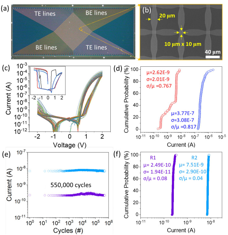
Ionic memristor devices are crucial for efficient artificial neural network computations in neuromorphic hardware. They excel in multi-bit implementation but face challenges like device reliability and sneak currents in crossbar array architecture (CAA). Interface-type ionic memristors offer low variation, self-rectification, and no forming process, making them suitable for CAA. However, they suffer from slow weight updates and poor retention and endurance. To address these issues, the study demonstrated an alkali ion self-rectifying memristor with an alkali metal reservoir formed by a bottom electrode design. By adopting Li metal as the adhesion layer of the bottom electrode, an alkali ion reservoir was formed at the bottom of the memristor layer by diffusion occurring during the atomic layer deposition process for the Na:TiO2 memristor layer. In addition, Al dopant was used to improve the retention characteristics by suppressing the diffusion of alkali cations. In the memristor device with optimized Al doping, retention characteristics of more than 20 h at 125 °C, endurance characteristics of more than 5.5 × 10⁵, and high linearity/symmetry of weight update characteristics were achieved. In reliability tests on 100 randomly selected devices from a 32 × 32 CAA device, device-to-device and cycle-to-cycle variations showed low variation values within 81% and 8%, respectively.

Keywords: adhesion layer; alkali cation; artificial neural networks; reservoir layer; synaptic response.


Conflict of interest statement

The authors declare no competing financial interest.

Figures

Figure 1
Figure 1
(a) Schematic representation of the Al,Na:TiO2in-situ ALD process. One supercycle consists of nTi cycles composed of TTIP and homemade reactant and 1Al cycle composed of TMA and homemade reactant. The amount of Al doping was controlled by adjusting the nTi:1Al ratio. (b) Schematic diagram (left) and cross-sectional bright field STEM image (right) of the self-rectifying alkali-ion memristor device. The device with Au (80 nm)/Li (5 nm)/Al,Na:TiO2 (18 nm)/Au (40 nm)/Li (5 nm) structure was fabricated on SiO2 (300 nm)/p-Si substrate. The Li adhesion layer and Li Na reservoir are marked in the device schematic and bright field STEM image as black and red arrows, respectively. (c) Schematic representation of in-situ ALD growth (left) and schematic band diagram (right) of Al,Na:TiO2. From the Li adhesion layer, Li diffuses over the bottom electrode and dopes into the bottom of the Al,Na:TiO2 film. The eight defect species that can be considered in this process are indicated by dotted boxes, p-type defects (LiTi’’’, AlTi, NaTi’’’), and n-type defects (Nai, Lii, Ali•••, Tii••••, VO••) indicated by blue and green dotted boxes, respectively. The p-type and n-type defects form energy levels at the bottom and top within the TiO2 bandgap, respectively, and shift the Fermi level in the CBM or VBM direction. The concentration of each defect species affects the direction of the Fermi level shift depending on the dominant species.
Figure 2
Figure 2
Dynamic SIMS depth profile results of (a) Al 0, (b) Al 3, (c) Al 6, and (d) Al 9/Au (40 nm)/Li (5 nm) samples. The yellow box in the figure indicates the bottom interfacial region of the Al,Na:TiO2 layer with the Au BE. (e) Schematic representation of three simplified surface species Ti-OH, Li-OH, and O-Li considering results by diffused Li. (f) O 1s and (g) Ti 2p XPS results of Al 0, Al 3, Al 6, and Al 9 samples. The dotted line and red arrow in the figures indicate the binding energy of the main peak in the Al 0 sample and the direction of the peak shift, respectively. (h) Schematic representation of the native oxygen vacancy present in TiO2 and (i) the passivation effect and additional oxygen vacancies created by Al doping (top) and the resulting band diagram (bottom). (Defects caused by alkali ions are excluded.)
Figure 3
Figure 3
Resistive switching properties (10 cycles of DC sweep curves) of (a) Al 0, (b) Al 3, (c) Al 6, and (d) Al 9 devices fabricated by 5 um × 5 um crosspoint structure and schematic band diagram (right) of each devices. Above and below the band schematic are labeled n-type defects (red) and p-type defects (blue) species, respectively. The n-type (red) and p-type (blue) defect species are labeled above and below the band diagram. (e) A schematic representation of the RS mechanism of the self-rectifying alkai-ion memristor. Here, both the top and bottom interfaces change their interface resistance by the redistribution of alkali ions. (f) Three-dimensional compositional distribution graph for elements O, Ti, Li, and Na from the surface to the bottom interface, constructed based on SIMS data of the Al 0 sample. (g) Expected band diagrams for each state: HRS@positive voltage (left); LRS@positive voltage (right).
Figure 4
Figure 4
Retention properties of (a) Al 0, (b) Al 3, (c) Al 6, and (d) Al 9 devices, measured by +1 V every 2 s at 125 °C, after fully switching to LRS and HRS using ±3 V DC sweep. (e) Warburg plots (ω–1/2 vs Zim) measured at room temperature for Al 0, Al 3, Al 6, and Al 9. The AW values marked on each plot are the Warburg coefficients obtained from the slopes. (f) Pulse width-dependent average change in conductance for Al 0, Al 3, Al 6, and Al 9 at 5 μs, 10 μs, 20 μs, 30 μs, and 50 μs. The average change in conductance was measured by employing pulses of varying widths (5 μs, 10 μs, 20 μs, 30 μs, and 50 μs) over 100 weight update cycles. For each cycle, conductance was measured using a read voltage of +1 V for potentiation, and the slope of 100 cycles of potentiation was used to determine the average conductance change.
Figure 5
Figure 5
Six cycles of LTP/LTD curves obtained from 1 device (left) and polar plots (pulse number vs conductance) for the LTP/LTD curves obtained from 20 different devices (right) of (a) Al 0, (b) Al 3, (c) Al 6, and (d) Al 9 devices. 256 weight updates were performed using ±5 V amplitude and 5 μs width of pulse train and read using +1 V at each step. Simulation results of 28 × 28 (e) digit and (f) fashion MNIST classification of Al 0, Al 3, Al 6, and Al 9 devices derived based on the long-term potentiation and depression curves obtained in (a)–(d).
Figure 6
Figure 6
(a) Optical microscope image of a 32 × 32 crossbar array device fabricated using Al 6. (b) SEM image of three magnified device cells in a 32 × 32 crossbar array device. (c) ±2 V DC sweep curves measured on randomly 100 selected devices. The inset is the DC curves of the three devices that experienced hard breakdown among the 100 devices. (d) A cumulative probability plot of HRS and LRS extracted at read voltage +1 V from 97 devices, excluding the 3 failed devices. (e) Endurance data measured 5.5 × 10⁵ times using switching condition pulse amplitude ±5 V, width 100 μs, and read condition +1 V (DC). (f) Cumulative probability plot extracted from endurance data for cycle-to-cycle variation.

Similar articles

Cited by

  • Memristive Ion Dynamics to Enable Biorealistic Computing.
    Zhao R, Kim SJ, Xu Y, Zhao J, Wang T, Midya R, Ganguli S, Roy AK, Dubey M, Williams RS, Yang JJ. Zhao R, et al. Chem Rev. 2025 Jan 22;125(2):745-785. doi: 10.1021/acs.chemrev.4c00587. Epub 2024 Dec 27. Chem Rev. 2025. PMID: 39729346 Free PMC article. Review.

References

    1. Sangwan V. K.; Lee H.-S.; Bergeron H.; Balla I.; Beck M. E.; Chen K.-S.; Hersam M. C. Multi-terminal memtransistors from polycrystalline monolayer molybdenum disulfide. Nature 2018, 554, 500–504. 10.1038/nature25747. - DOI - PubMed
    1. Auciello O.; Scott J. F.; Ramesh R. The Physics of Ferroelectric Memories. Phys. Today 1998, 51, 22–27. 10.1063/1.882324. - DOI
    1. Mathews S.; Ramesh R.; Venkatesan T. Ferroelectric Field Effect Transistor Based on Epitaxial Perovskite Heterostructures. Science 1997, 276, 238–240. 10.1126/science.276.5310.238. - DOI - PubMed
    1. Lee J.; Choi S.; Lee C.; Kang Y.; Kim D. GeSbTe deposition for the PRAM application. Appl. Surf. Sci. 2007, 253, 3969–3976. 10.1016/j.apsusc.2006.08.044. - DOI
    1. Li Z.; Zhang S. Domain-wall dynamics driven by adiabatic spin-transfer torques. Phys. Rev. B 2004, 70, 024417.10.1103/PhysRevB.70.024417. - DOI - PubMed