

Nanoscale morphology, optical dynamics and gas sensor of porous silicon
- PMID: 38355956
- PMCID: PMC10866982
- DOI: 10.1038/s41598-024-54336-x
Nanoscale morphology, optical dynamics and gas sensor of porous silicon
Abstract
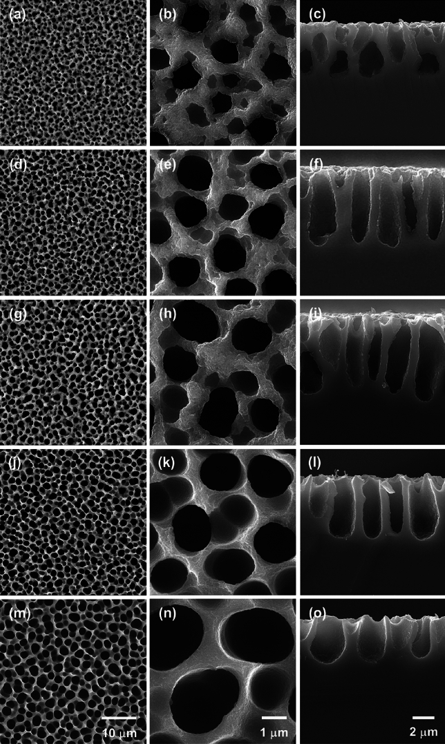
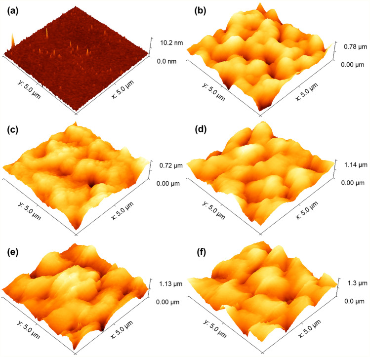
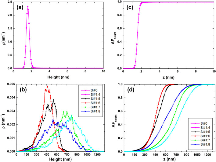
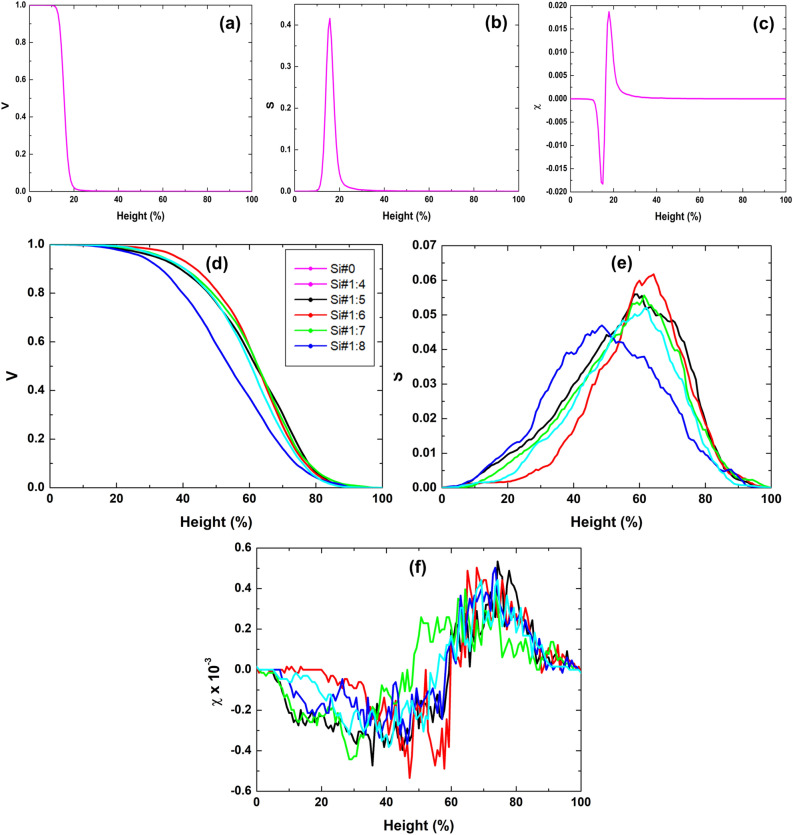
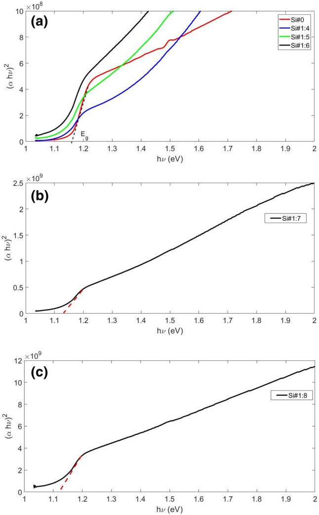
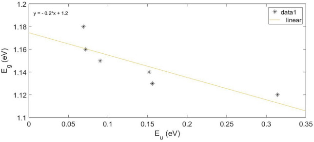
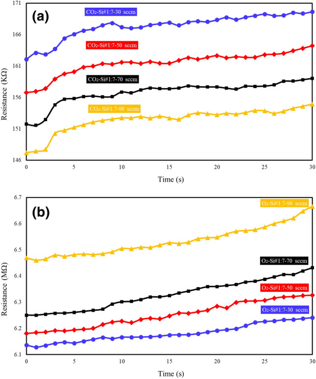
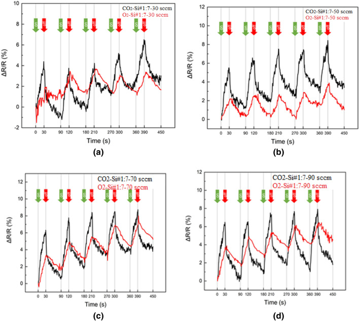
We investigated the multifaceted gas sensing properties of porous silicon thin films electrodeposited onto (100) oriented P-type silicon wafers substrates. Our investigation delves into morphological, optical properties, and sensing capabilities, aiming to optimize their use as efficient gas sensors. Morphological analysis revealed the development of unique surfaces with distinct characteristics compared to untreated sample, yielding substantially rougher yet flat surfaces, corroborated by Minkowski Functionals analysis. Fractal mathematics exploration emphasized that despite increased roughness, HF/ethanol-treated surfaces exhibit flatter attributes compared to untreated Si sample. Optical approaches established a correlation between increased porosity and elevated localized states and defects, influencing the Urbach energy value. This contributed to a reduction in steepness values, attributed to heightened dislocations and structural disturbances, while the transconductance parameter decreases. Simultaneously, porosity enhances the strength of electron‒phonon interaction. The porous silicon thin films were further tested as effective gas sensors for CO2 and O2 vapors at room temperature, displaying notable changes in electrical resistance with varying concentrations. These findings bring a comprehensive exploration of some important characteristics of porous silicon surfaces and established their potential for advanced industrial applications.
Keywords: Gas sensor performance; Morphological properties; Optical properties; Porous silicon; Thin films.
© 2024. The Author(s).
Conflict of interest statement
The authors declare no competing interests.
Figures

Similar articles
-
NH3 sensing characteristics of nano-WO3 thin films deposited on porous silicon.J Nanosci Nanotechnol. 2010 Nov;10(11):7739-42. doi: 10.1166/jnn.2010.2815. J Nanosci Nanotechnol. 2010. PMID: 21138022
-
Effect of thickness on nanostructured SnO2 thin films by spray pyrolysis as highly sensitive H2S gas sensor.J Nanosci Nanotechnol. 2012 Aug;12(8):6192-201. doi: 10.1166/jnn.2012.6424. J Nanosci Nanotechnol. 2012. PMID: 22962726
-
Surface morphology-dependent room-temperature LaFeO₃ nanostructure thin films as selective NO₂ gas sensor prepared by radio frequency magnetron sputtering.ACS Appl Mater Interfaces. 2014 Aug 27;6(16):13917-27. doi: 10.1021/am503318y. Epub 2014 Jul 23. ACS Appl Mater Interfaces. 2014. PMID: 25029197
-
Porous Silicon Structures as Optical Gas Sensors.Sensors (Basel). 2015 Aug 14;15(8):19968-91. doi: 10.3390/s150819968. Sensors (Basel). 2015. PMID: 26287199 Free PMC article. Review.
-
Big Potential From Silicon-Based Porous Nanomaterials: In Field of Energy Storage and Sensors.Front Chem. 2018 Nov 8;6:539. doi: 10.3389/fchem.2018.00539. eCollection 2018. Front Chem. 2018. PMID: 30467539 Free PMC article. Review.
Cited by
-
A Comparison of the Electrical Properties of Gel Polymer Electrolyte-Based Supercapacitors: A Review of Advances in Electrolyte Materials.Gels. 2024 Dec 6;10(12):803. doi: 10.3390/gels10120803. Gels. 2024. PMID: 39727559 Free PMC article. Review.
-
Silver Nanoparticles-Decorated Porous Silicon Microcavity as a High-Performance SERS Substrate for Ultrasensitive Detection of Trace-Level Molecules.Nanomaterials (Basel). 2025 Jun 30;15(13):1007. doi: 10.3390/nano15131007. Nanomaterials (Basel). 2025. PMID: 40648714 Free PMC article.
References
-
- Uhlir A. Electrolytic shaping of germanium and silicon. Bell. Syst. Tech. J. 1956;35:333–347. doi: 10.1002/j.1538-7305.1956.tb02385.x. - DOI
-
- Lachenani H, Larabi A, Gabouze N. Study of structural, electronic and vibrational properties of porous silicon with different porosity. Silicon. 2019;11:2505–2515. doi: 10.1007/s12633-019-00137-1. - DOI
-
- Solaymani S, Ghaderi A, Dejam L, Garczyk Z, Sapota W, Stach S, Dalouji V, Luna C, Elahi SM, Elahi SH. Correlation between the multifractal structure, crystalline and photoluminescence properties of engineered CZO thin films. Int. J. Hydrog. Energy. 2017;42:20. doi: 10.1016/j.ijhydene.2017.04.045. - DOI
-
- Praveenkumar S, Lingaraja D, Mahiz Mathi P, Dinesh Ram G. An experimental study of optoelectronic properties of porous silicon for solar cell application. Optik (Stuttg). 2019;178:216–223. doi: 10.1016/j.ijleo.2018.09.176. - DOI
-
- Dalouji V, Elahi SM, Ghaderi A, Solaymani S. Influence of annealing temperature on berthelot-type hopping conduction mechanism in carbon-nickel composite films. Chin. Phys. Lett. 2016;33:5. doi: 10.1088/0256-307X/33/5/057203. - DOI
LinkOut - more resources
Full Text Sources
Research Materials
Miscellaneous
