

The Roadmap of 2D Materials and Devices Toward Chips
- PMID: 38363512
- PMCID: PMC10873265
- DOI: 10.1007/s40820-023-01273-5
The Roadmap of 2D Materials and Devices Toward Chips
Abstract
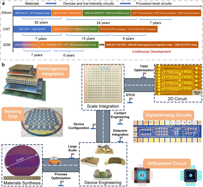
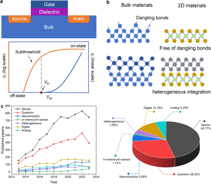
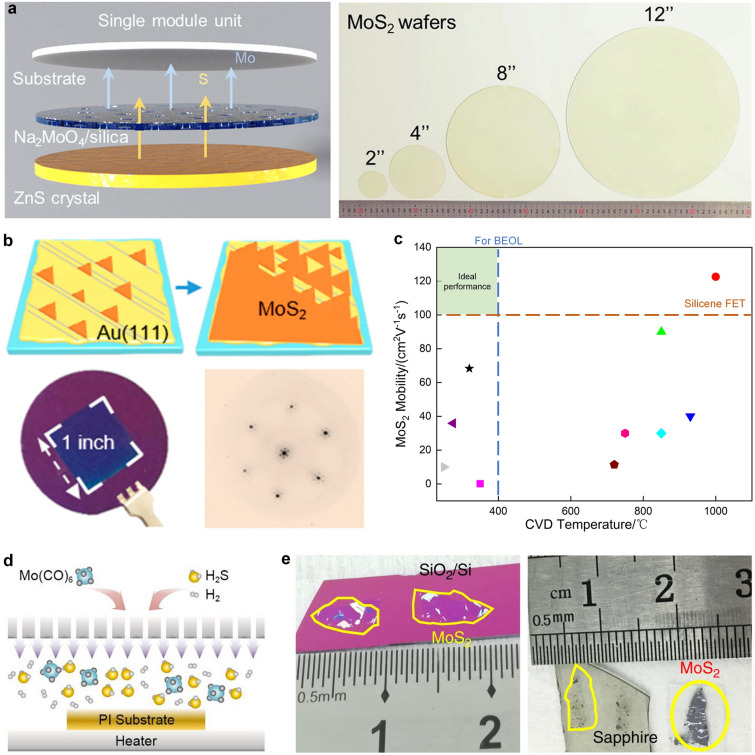
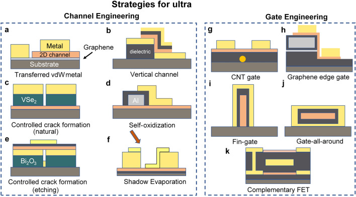
Due to the constraints imposed by physical effects and performance degradation, silicon-based chip technology is facing certain limitations in sustaining the advancement of Moore's law. Two-dimensional (2D) materials have emerged as highly promising candidates for the post-Moore era, offering significant potential in domains such as integrated circuits and next-generation computing. Here, in this review, the progress of 2D semiconductors in process engineering and various electronic applications are summarized. A careful introduction of material synthesis, transistor engineering focused on device configuration, dielectric engineering, contact engineering, and material integration are given first. Then 2D transistors for certain electronic applications including digital and analog circuits, heterogeneous integration chips, and sensing circuits are discussed. Moreover, several promising applications (artificial intelligence chips and quantum chips) based on specific mechanism devices are introduced. Finally, the challenges for 2D materials encountered in achieving circuit-level or system-level applications are analyzed, and potential development pathways or roadmaps are further speculated and outlooked.
Keywords: Integrated circuits; Post-Moore era; Roadmap; Two-dimensional materials.
© 2024. The Author(s).
Conflict of interest statement
The authors declare no interest conflict. They have no known competing financial interests or personal relationships that could have appeared to influence the work reported in this paper. He Tian is an editorial board member for Nano-Micro Letters and was not involved in the editorial review or the decision to publish this article. All authors declare that there are no competing interests.
Figures


References
-
- J.S. Kilby, Invention of integrated-circuit. IEEE Tran. Electron. Devices 23(7), 648–654 (1976). 10.1109/t-ed.1976.18467
-
- K. Uchida, H. Watanabe, A. Kinoshita, J. Koga, T. Numata et al., Experimental study on carrier transport mechanism in ultrathin-body SOI n- and p-MOSFETs with SOI thickness less than 5 nm. in 2002 IEEE International Electron Devices Meeting (IEDM), San Francisco, CA, USA, 47–50 (2002). 10.1109/IEDM.2002.1175776
-
- D.J. Frank, R.H. Dennard, E. Nowak, P.M. Solomon, Y. Taur et al., Device scaling limits of Si MOSFETs and their application dependencies. Proc. IEEE 89(3), 259–288 (2001). 10.1109/5.915374
-
- S. Zeng, Z. Tang, C. Liu, P. Zhou, Electronics based on two-dimensional materials: Status and outlook. Nano Res. 14, 1752–1767 (2021). 10.1007/s12274-020-2945-z
-
- D.E. Nikonov, I.A. Young, Overview of beyond-CMOS devices and a uniform methodology for their benchmarking. Proc. IEEE 101(12), 2498–2533 (2013). 10.1109/jproc.2013.2252317
Publication types
LinkOut - more resources
Full Text Sources