Review
. 2024 Mar 5;18(9):6766-6816.
doi: 10.1021/acsnano.3c10412. Epub 2024 Feb 20.

Atomically Precise Manufacturing of Silicon Electronics

Affiliations
Review

Atomically Precise Manufacturing of Silicon Electronics

Jason Pitters et al. ACS Nano. .

Abstract

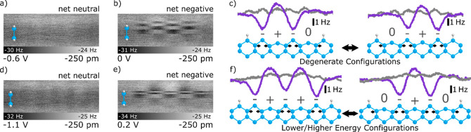
Atomically precise manufacturing (APM) is a key technique that involves the direct control of atoms in order to manufacture products or components of products. It has been developed most successfully using scanning probe methods and has received particular attention for developing atom scale electronics with a focus on silicon-based systems. This review captures the development of silicon atom-based electronics and is divided into several sections that will cover characterization and atom manipulation of silicon surfaces with scanning tunneling microscopy and atomic force microscopy, development of silicon dangling bonds as atomic quantum dots, creation of atom scale devices, and the wiring and packaging of those circuits. The review will also cover the advance of silicon dangling bond logic design and the progress of silicon quantum atomic designer (SiQAD) simulators. Finally, an outlook of APM and silicon atom electronics will be provided.

Keywords: atomic electronics; atomic force microscopy; atomic quantum dot; atomic scale devices; atomically precise manufacturing; dangling bond; hydrogen terminated silicon; scanning tunneling microscopy; silicon quantum atomic designer.


Conflict of interest statement

The authors declare no competing financial interest.

Figures

Figure 1
Figure 1
Ball and stick model and STM image of H terminated silicon 100 (2×1). Silicon atoms in yellow and hydrogen atoms in white. Each ball-like structure in the STM image derives from a silicon atom terminated with a hydrogen atom. Dimensions between silicon atoms are shown in the image.
Figure 2
Figure 2
Different STM imaging modes of the same sample area of H-terminated silicon. (a) STM constant-current empty states image (V = 1.3 V, I = 50 pA). (b) STM constant-current filled states image. (c) STM constant-height image of the same area. (V = 300 mV, zrel = −300 pm). A pronounced “X” shaped feature due to a near surface dopant becomes clear at these imaging conditions. All images are 25 × 25 nm2 in area, and zrel is a measure of the relative tip–sample height as referenced to a known STM set-point of V = −1.8, I = 50 pA over a hydrogen atom. Reprinted with permission from ref (48). Copyright 2020 Taleana Huff.
Figure 3
Figure 3
(a and b) Scanning tunneling spectra (STS) of hydrogen terminated silicon. The sample was prepared by flash annealing to (a) 1050 °C followed by hydrogen termination. After STS measurement the sample was flash annealed to (b) 1250 °C followed by hydrogen termination. Colors indicate the displaced tip height from the tunneling set point of −2 V, 0.1 nA. Red arrows indicate the location of the valence band onset. It is shifted for the 1250 °C sample. The black arrow indicates the tunneling current resulting from dopant states that are only observed for 1050 °C heated samples. (c–f) SIMS data showing arsenic levels in samples prepared with various annealing methods. Control 1 and 2 experience no high temperature heating. Sample 3 was heated to 1050 °C two times. Sample 4 was heated to 1050 more than 10×. Samples 5 and 6 were heated to 1250 °C two times and greater than ten times, respectively. Dopant levels are depleted significantly for all samples flashed to 1250 °C and for depths over 150 nm. (g) Shows a schematic of the silicon band diagram (not to scale) with varying dopant density according to the SIMS profile, consistent with the observation of a Fermi level within the gap in the near surface region and above the conduction band in the bulk. Reprinted with permission from ref (53). Copyright 2012 American Vacuum Society.
Figure 4
Figure 4
Illustration of the STM setup used to measure atomically resolved subsurface dopant images. A phosphorus atom is found a few nanometers below the surface of silicon (100) 2×1 and is highlighted in red in (c). Simulated and experimental STM images of the buried dopant are shown. Reprinted by permission from ref (50). Copyright 2016 Springer Nature. www.nature.com/nnano/.
Figure 5
Figure 5
Constant-height AFM probing of H:Si at different heights with a hydrogen passivated tip. (a) Empty states STM image (V = 1.3 and I = 50 pA) of a 3 × 3 nm2 area of H:Si(100) 2×1. (b) Δf(z) spectra taken over top of a hydrogen atom. The spectra location is marked in (a). zrel = 0 pm is referenced to an STM set-point of I = 50 pA with V = −1.8 V over top of a hydrogen atom. (c–n) Constant-height AFM Δf maps of the same 3 × 3 nm2 area taken at different heights. Heights are listed in the lower right corner of every image (V = 0 V and Osc.Amp = 50 pm) and are also marked in (b). Reprinted with permission from ref (48). Copyright 2020 Taleana Huff.
Figure 6
Figure 6
Electrostatic shift from charged defects. (a) Δf(V) spectroscopies over a subsurface Arsenic dopant (red, VCPD = −0.53 V), a proposed Si vacancy (blue, VCPD = −0.46 V), and the H-Si surface (green, VCPD = −0.50 V) as shown in the empty states STM image in (b). The image was acquired at Vs = 1.3 V and Iset = 50 pA. Spectra in (a) taken at zrel = 0 pm. The inset of (b) shows a constant-height image of the arsenic dopant, better highlighting the electronic properties from the bulk (Vs = 0.4 V, Zrel = −200 pm).
Figure 7
Figure 7
Common surface defects on the H-Si(100)-2×1 surface. (a) Empty states STM and (b) nc-AFM images of the 3×1 surface reconstruction. (c) Empty states STM and (d) nc-AFM images of the 1×1 surface reconstruction (dihydride pair). (e) Empty states STM and (f) nc-AFM images of a single dihydride defect. (g) Empty states STM and (h) nc-AFM images of a siloxane dimer defect. STM images are acquired at Vs = 1.3 V and Iset = 50 pA. nc-AFM images are acquired at Vs = 0 V and Zrel = −400 pm ((d) Zrel = −480 pm). Each image is 2.2 × 2.2 nm2. Reproduced from ref (114) (https://doi.org/10.3762/bjnano.11.11. Copyright 2020 Jeremiah Croshaw et al., published by Beilstein-Institut, distributed under the terms of the Creative Commons Attributions 4.0 International License. https://creativecommons.org/licenses/by/4.0).
Figure 8
Figure 8
Molecular model of an isolated DB in its neutral state. (a) An isosurface (with color phase) of the HOMO, i.e. the neutral DB0 orbital, along the [−110] direction. (b) The same DB0 isosurface (solid color) seen from the [110] direction compared to the LUMO, i.e. the virtual DB0 state depicted as a mesh, which is also found in the bandgap of the bulk silicon. (c) Top view (along the [001] direction) of the same isosurface. Calculations were performed on a H-terminated silicon nanocluster having 8 Si layers in the z-direction and 4×8 surface unit cells in the xy-plane.
Figure 9
Figure 9
DB energy levels in an H:Si nanocluster containing a single DB. (a) A neutral DB has a singly occupied spin-polarized orbital 40 meV above the reference level (red dashed line) of the nanocluster and a virtual orbital higher in energy. (b) A negative DB has a doubly occupied (spin-paired) orbital 610 meV higher than the reference level.
Figure 10
Figure 10
Qualitative band diagrams for the DB levels with and without the imaging probe and associated band bending. (a) Unperturbed neutral DB case with no band bending at the surface and the charge transition levels depicted in the band gap. (b) The CTLs in the presence of an external STM imaging probe. EFtip and EFSi label the tip and sample chemical potentials, respectively, and Γ labels filling and emptying processes. CBM and VBM stand for conduction band minimum and valence band maximum of bulk silicon. Reprinted with permission from ref (117). Copyright 2014 American Physical Society. https://doi.org/10.1103/PhysRevLett.112.256801.
Figure 11
Figure 11
Typical STM images of a single DB in the (a) empty-state imaging, 40 pA, +2 V; and (b) and filled-state imaging, 40 pA, −2 V. (c and d) Cross sections through the indicated dashed lines in each image. Reprinted with permission from ref (158). Copyright 2015 Marco Taucer.
Figure 12
Figure 12
(a) Charge transfer mechanisms between the STM tip, DB, and silicon. The DB is marked as purple, Si atoms in green, and H atoms in white. (b,c) Band diagram representations of those mechanisms. (d) Electrostatic potential landscape at the tip-vacuum-silicon interface calculated self-consistently by solving the Poisson–Schrödinger equation in the semiclassical approximation. Reprinted in part with permission from ref (159). Copyright 2011 by the American Physical Society. https://doi.org/10.1103/PhysRevB.84.205416.
Figure 13
Figure 13
Reactions of hydrogen atoms after HDL. (a) STM image after HDL with constant dose, variable pattern size. (b) Average number of spurious DBs as a function of pattern size for two separate tips. (c) STM image of a single hydrogen atom (indicated with yellow arrow) physisorbed on the surface after DB formation (1.3 V, 5 nm × 5 nm). (d) Close up of physisorbed H, 1.3 V, 3 nm × 3 nm. However, when the scanning voltage is increased to V = 1.7 V in (e), the hydrogen atom is dragged by the tip and moved close enough to the DB to cap it, as indicated by a change in contrast midway through the image and confirmed by a subsequent STM image of the same area (f). (e) and (f) are larger area 10 × 10 nm images of the area in (c). Reprinted in part with permission from ref (121). Copyright 2018 Springer Nature BV. Reproduced from ref (144) with the permission of AVS: Science & Technology of Materials, Interfaces, and Processing. https://doi.org/10.1116/1.4864302.
Figure 14
Figure 14
Procedure to mechanically induce a hydrogen–silicon covalent bond. (a) Typical filled-state STM image of a silicon dangling bond on the H-Si(100) surface using a single hydrogen atom functionalized tip. The yellow arrow indicates a defect taken as a reference. (b) Δf(z) curve using a H-functionalized tip on a surface hydrogen atom. (c) Ball-and-stick model and (d) Δf(z) curve on a single DB during the mechanically induced Si–H covalent bond capping event. The orange arrow indicates a hysteresis (zoom on inset) characteristic of the change that occurs due to the formation of the Si–H bond. (e) STM image and (f) Δf(z) curve on the Si–H surface subsequent to the mechanically induced reaction in (d). Reprinted with permission from ref (199). Copyright 2017 American Chemical Society.
Figure 15
Figure 15
Tunneling current signatures of hydrogen repassivation. (a) (V = 0.4 V, T = 4.5 K) The recorded tunneling current as the scanning tunneling microscope (STM) tip (set over a dangling bond (DB) at 1.4 V and 50 pA) is brought toward the surface (blue) and as the STM tip is retracted (red) during hydrogen repassivation (HR). (b) (V = 0.2 V) A second distinct signature (type-II) has also been observed during HR, with a sudden decrease in tunneling current during the approach toward the surface (blue). (c) The tip approach distance where either signature occurred was recorded for 119 unique HR events. Nearly 90% of events occur before 550 pm. The inset depicts the STM tip approaching a DB on the surface. Used with permission of Springer Nature BV from ref (201). Copyright 2018; permission conveyed through Copyright Clearance Center, Inc.
Figure 16
Figure 16
Hydrogen molecule reacting with an interdimer site of H-Si(100) at 4 K. (a) Ball and stick diagram. (b) Interdimer site is observed. (c) After exposure to hydrogen gas at 4 K, the interdimer site is capped. Reprinted in part with permission from ref (202). Copyright 2020 American Chemical Society.
Figure 17
Figure 17
STM images of hydrogen desorption patterns on Si(100)-H. Perfect desorption patterns were not achieved. From ref (15). Copyright 1995. Reprinted in part with permission from AAAS. https://doi.org/10.1126/science.268.5217.1590. Reproduced from ref (177). Copyright 2010, with the permission of AIP Publishing. Reprinted in part with permission from ref (205). Copyright 1998 Springer Nature. Reprinted in part from ref (206). Copyright (2006), with permission from Elsevier.
Figure 18
Figure 18
Some mass desorption patterns from dedicated hardware systems with tunneling and field emission desorption and for qubit manufacturing. (a) shows hydrogen desorption in low bias tunneling and high bias field emission regimes. (b and c) show various aligned patterns and patterns created from improved scanner control at different scales. (d) shows the controlled H desorption pattern for quantum dot and electrode formation. Reprinted in part with permission from ref (211). Copyright 2018, with permission from Elsevier. https://doi.org/10.1016/j.mne.2018.11.001. Reprinted in part with permission from ref (209). Copyright 2019 Springer Nature. https://doi.org/10.1038/s41586-019-1381-2.
Figure 19
Figure 19
Plot of the patterning parameters for single-dimer-row hydrogen desorption. The region between the two dashed lines provides optimal single-dimer-row lithography. Measurements were performed using three different W tips. Patterning parameters used by other groups are shown for comparison (see reference for details within). Inset bottom: a typical single-dimer-row wire patterned with the optimized condition of 3 V, 30 nA, 10 mC cm–1. Inset top: a typical TEM image of the sharpening tip. Adapted with permission from ref (212). Copyright 2012 IOP Publishing Ltd. https://doi.org/10.1088/0957-4484/23/27/275301.
Figure 20
Figure 20
Perfect patterns form lines/wires in (a) and artificial molecules in (b) and (c). Error correction allows for more complex structures as shown in (d). Reprinted in part with permission from ref (149). Copyright 2013 Springer Nature. https://doi.org/10.1038/ncomms2679. Used with permission of Springer Nature BV from ref (201). Copyright 2018; permission conveyed through Copyright Clearance Center, Inc. Reprinted in part with permission from ref (216). Copyright 2013 American Physical Society. https://doi.org/10.1103/PhysRevLett.82.4034. Reprinted in part with permission from ref (217). Copyright 2018 American Chemical Society.
Figure 21
Figure 21
Autonomous tip sharpening used along with atom-scale patterning. (a) An overview (25 × 25 nm2) STM image showing a patterned binary atomic wire, an isolated DB used for tip quality assessment, and a spot (red cross) chosen by the user to perform tip conditioning. (b) Sequence of patterning steps without noticeable tip quality change in between. (c) The tip became double after the creation of the last atom on the right, and the user employed the tip conditioning routine to resharpen it. After three steps of automatic tip conditioning, the tip became sharp and the user carried on the pattering (d). (e) STM images of the isolated DB at the middle left of (a) after each tip conditioning. The CNN used these images to assess the quality of the tip. (f) Output of the CNN for the images in (e). The tunneling conditions were −1.8 V and 50 pA for all images. Reprinted with permission from ref (218). Copyright 2018 American Chemical Society.
Figure 22
Figure 22
(a) A trace of the defects from the CNN analysis of the scan image shown. The white square shows the area furthest from defects for the corresponding pattern. (b) The resulting surface after patterning the device shown in the inset. Reprinted with permission from ref (219). Copyright 2020 IOP Publishing Ltd. https://doi.org/10.1088/2632-2153/ab6d5e.
Figure 23
Figure 23
(a) Topographical STM image of a single DB taken with V = 1.4 V and I = 20 pA. The double-ended arrow shows the range of lateral positions used to acquire the data shown in (a). (b) Histogram of current measurements with the tip at a constant height and a constant voltage of 1.45 V positioned 3.14 nm from the DB. The peak at lowest current corresponds to the negative charge state, while the peaks at intermediate and highest current correspond to the neutral and positive charge states. (c) An example of a current–time trace. The sampling rate is 10 kHz and the entire trace (not shown) is 2 s in length. Reprinted with permission from ref (117). Copyright 2014 American Physical Society. https://doi.org/10.1063/1.111722.
Figure 24
Figure 24
(a), (b), and (c): 10 × 10 nm2 constant-current (30 pA) STM images of a single DB at +1.6 V, −1.8 V, and −1.7 V, respectively. (d) I/V (blue curve) and dI/dV (red curve) spectroscopy of the same DB. (e) dI/dV spectroscopies of a single DB (red curve) and Si:H surface (black curve). (f) Statistics over 69 DBs showing the variation of the charge-state transition peak voltage onset. Reprinted with permission under a Creative Commons CC BY 3.0 License from ref (220). Copyright 2015 IOP Publishing Ltd. https://creativecommons.org/licenses/by/3.0/.
Figure 25
Figure 25
(a) Calculated I(V) spectra of a single silicon dangling bond at different tip–sample distances using NEGF (colors are used for clarity). (b)–(e) Energy diagrams of the system of study for all the different energy regimes observed in the I(V) spectra. The Fermi energies of the bulk silicon (EFSi) and the tip (EFtip) as well as the DB charge transition levels, (+/0) and (0/−), are displayed in the diagram. (b) The tip Fermi level is above both the DB charge transition levels. (c) The tip Fermi level is in resonance with the (0/−) level and above the (+/0) level. (d) The tip Fermi level is in resonance with the (+/0) level. (e) The tip Fermi level is below both charge transition levels, and due to tip induced band bending, the (+/0) level becomes resonant with the bulk valence band edge. Reprinted with permission from ref (222). Copyright 2016 American Physical Society. https://doi.org/10.1103/PhysRevLett.117.276805.
Figure 26
Figure 26
(a) KPFM (red) and NDR I(V) (black) curves measured for a DB on a 1250 °C annealed sample. The KPFM curve was measured at z = −330 pm from the reference height of −1.80 V and 50 pA, set over hydrogen. The oscillation amplitude was 100 pm. Two features in the KPFM curve are visible (indicated by red arrows) which correspond to the (0/−) charge transition level (approximately −0.20 V) and the (+/0) charge transition level (approximately −1.10 V). (b) T(+/0)b time constant of DBs on samples annealed at different temperatures (1250 and 1050 °C) during preparation. (c) T(+/0)b vs tip height offset measured for a DB on an n-type sample annealed at 1250 °C during preparation. Initial tip height was set at −1.80 V and 50 pA on top of the DB. The time constants are measured at the sample bias of −1.45 V. Reprinted with permission from ref (65). Copyright 2017 American Chemical Society.
Figure 27
Figure 27
Δf(V) Spectroscopy over Hydrogen and a discrete-charge-state-changing dangling bond. (a) Δf(V) curve (black) taken by an AFM sensor over the center of a surface hydrogen atom on H:Si(100) (zrel = 0.0 pm, Vrange = −0.8 to 0.35 V, and Osc.Amp. = 50 pm). The data has been fitted with a parabolic curve (blue). The maximum of the fit (−0.53 ± 0.02 V) is marked with a pink dot. (b) Δf(V) curve (black) taken by an AFM sensor over the center of a dangling bond on H:Si(100) (zrel = −300 pm, Vrange = −0.8 to 0.35 V, and Osc.Amp. = 50 pm). For voltages in the orange shaded area, the DB is neutral. For voltages in the blue shaded area, the DB gains a single extra electron and is negative. The transition from neutral to negative, or the (0/−) charge transition step, is seen at V = −0.25 ± 0.01 V. Parabolic fits were done for both the neutral (orange) and positive (blue) charge states of the DB. Values of V* could be extracted from the fits for the two charge states, highlighting how even a single electron change can drastically affect the measured CPD offset. Reprinted in part with permission from ref (49). Copyright 2019 American Chemical Society.
Figure 28
Figure 28
Probing charged species with a movable DB point-probe. (a–g) Constant-height STM images of the DB being moved 0–6 lattice sites away from its initialization point, respectively, from a near-surface arsenic atom (Zrel = −250 pm and V = 300 mV). (h) Constant-height STM image of the area before addition of a DB, with Δf(V) locations marked (Zrel = −200 pm and V = 250 mV). (i) Δf(V) spectroscopy taken on top of the DB for each lattice spacing, color coded with the positions in (h), as well as with the frames in (a–g) (Zrel = −350 pm). Reprinted in part with permission from ref (49). Copyright 2019 American Chemical Society.
Figure 29
Figure 29
Varied CPD in small scan areas. (a) Constant-height STM image (V = 300 mV) of a subsurface arsenic dopant (appears as the bright feature in the upper left portion of the image) and an unknown charged species (appears dark in the lower right region), now thought to be a Si Vacancy.) (b) Constant-current STM image (V = 1.3 V, I = −50 pA) of the same area. (c) KPFM difference map compared to the unperturbed surface (25 × 25 nm2 grid, voltage range −1.8 V to −1.0 V. All scale bars are 5 nm. Reprinted in part with permission from ref (49). Copyright 2019 American Chemical Society.
Figure 30
Figure 30
(Si dimers = blue, H = white, subsurface Si = gray). (a) RT STM image of low doped n-type Si (∼5 × 1015 cm–3). 35 × 35 nm2, 2 V, 0.1 nA. DBs appear bright. (b) High doped n-type Si (∼5 × 1018 cm–3). 35 × 35 nm2, 2.2 V, 0.1 nA. DBs appear dark with a central spot. (c) 9 × 9 nm2, 2 V, 0.2 nA. Three groups of DBs are prepared. A noncoupled DB pair at 2.32 nm (I). Coupled DB pairs at 1.56 nm (II) and 1.15 nm (III). (d) Calculated one- and two-electron occupation probabilities (black and red curves, respectively) corresponding to the DB pairs in (c). (e,f) Two groups of four spaced at various distances (schematics show the DB positions with respect to the silicon lattice). More closely spaced DBs have a reduced total charge and appear brighter compared to DBs spaced at further distances. (g) Occupation probabilities of a square four-DB structure in the absence of an STM imaging tip as a function of DB–DB separation along the square side. The legend indicates the corresponding symbols for the total number of electrons in the structure, from which the subtraction of 4 yields the number of extra electrons. (h) Group of four DBs spaced greater than 3.5 nm. All four DBs are negatively charged. Reproduced in part from ref (153). Copyright 2011, with the permission of AIP Publishing. Reproduced in part from ref (230). Copyright 2009 American Physical Society. https://doi.org/10.1103/PhysRevLett.102.046805.
Figure 31
Figure 31
A color mapped STM image (6 × 6 nm2, 2.5 V, 0.11 nA) of a rectangular 4-DB coupled entity with two additional electrostatically perturbing DBs diagonally placed. The 2 DBs nearest the negative perturbing DBs are relatively high in appearance as a result of unfavored electron occupation at those sites. The average height difference between the violet (higher) and blue colored (lower) DBs is ∼0.4 Å. A grid represents the DB positions on the silicon surface. Reprinted with permission from ref (230). Copyright 2009 American Physical Society. https://doi.org/10.1103/PhysRevLett.102.046805.
Figure 32
Figure 32
Characterizing charge occupations (V = −1.6 V, I = 50 pA, T = 4.5 K, 6.4 × 6.4 nm2). (a) STM image of a DB on the hydrogen-passivated Si(100)-2×1 surface. The DB (DB1) exhibits a sharp current onset in its I(V) spectrum (blue) due to the ionization of a subsurface arsenic dopant atom caused by the STM tip field. (b) A second DB (DB2), containing a net charge of one electron is added to the surface 5.4 nm away from DB1, causing the step in the I(V) spectrum of DB1 to shift to the left (f, dark green). (c) A third DB (DB3) is added near DB2, and no shift in the I(V) spectrum of DB1 is observed (f, light green). (d, e) The distance between DB2 and DB3 is varied to determine the net charge in the structure for each case. (f) The I(V) spectra taken over DB1, associated with (a–e), showing the sharp onset of current. Reprinted with permission from ref (202). Copyright 2020 American Chemical Society.
Figure 33
Figure 33
STM and AFM images of two DBs with various separations. (a–f) STM images ((a–c, V = 1.3 V, I = 50 pA, T = 4.5 K, 3 × 3 nm2) ((d–f), V = −1.8 V, I = 50 pA, T = 4.5 K, 3 × 3 nm2). (g–i) Constant-height AFM frequency shift images (V = 0 V, Zrel = −300 pm, T = 4.5 K, 3 × 3 nm2). The dark depressions in AFM represent the location of an electron within each structure. In (g) and (h) there is only a net charge of one additional electron within the structures. In (i) there are two net additional electrons present. STM and AFM. Reprinted in part with permission from ref (202). Copyright 2020 American Chemical Society.
Figure 34
Figure 34
Evolution of charge configurations with controlled preparation of a symmetric DB structure. Visualization of scan modes: (a) The tip is scanned from left to right in the read regime only. (b) The tip is scanned from left to right in the write regime only. (c) The tip is first scanned from left to right in the write regime, then scanned in the read regime from right to left. (d) The tip is first scanned from right to left in the write regime, then scanned in the read regime from left to right. (e) Constant-height Δf image of the six-DB structure. (f, g) Line scan maps across the structure in (e) corresponding to scheme (a) shown in (f), (b) shown in (g), (c) shown in (h), and (d) shown in (i). (f), (h), and (i) were measured in the read regime: −270 pm. (g) was measured in the write regime: −320 pm. Scale bar in (e) corresponds to 3 nm. All measurements taken at 0 V. Reprinted in part with permission from ref (234). Copyright 2018 American Physical Society. https://doi.org/10.1103/PhysRevLett.121.166801.
Figure 35
Figure 35
Manipulation of the DB charge state. (a) By adjusting the crystal doping level, the alignment of the sample Fermi level (EF) shifts relative to the DB(0/−) and DB(+/0), putting the DB in a positive (+), neutral (0), or negative (−) charge state (transition positions are illustrative). (b) Patterning a DB next to a fixed negative defect (red) shifts the local bands upward, bringing the DB(0/−) above the EF and putting the DB in a neutral charge state. (c) By positioning a probe tip near the DB, it enables electrons to tunnel from the DB into the tip. If the emptying rate to the tip is faster than the filling rate from the bulk, then the DB will sit in a neutral charge state.
Figure 36
Figure 36
Binary atomic silicon logic. (a, c, e, g, i) Constant-height Δf images of isolated left (a), isolated right (c), coupled pair (e), biased right (g), and biased left (i) DB assemblies. (b, d, f, h, j) Δf(V) spectra over each of the corresponding DB assemblies. (k) Experimentally measured (red) and TIBB corrected (blue) energy levels of the DB(0/−) transition levels of the DB assemblies. Reprinted in part with permission ref (121). Copyright 2018 Springer Nature BV.
Figure 37
Figure 37
AFM images of bit propagation in a binary wire. (a) 8 DB pair wire biased by a single negative DB (red dot) on the right. All DB pairs have charge shifted to the left, indicated by the binary number “0” (black dots). (b) The lone negative DB (red) is converted to a pair. The line of 9 DB pairs has a break located near the middle. (c) The 9 DB pair wire is then biased from the left by a single negative DB (red dot). The 9 DB pair wire is converted to all “1”s with the charge to the right side of the DB pair. Reprinted in part with permission from ref (121). Copyright 2018 Springer Nature BV.
Figure 38
Figure 38
OR gate constructed from binary pairs. A two input OR gate in (a) the uninitialized state, (b) the initialized state, (c) the “10” input state, (d) the “01” input state, and (e) the “11” input state. (f–j) Corresponding models of the AFM images indicating the presence or absence of any perturbing DB (red) and the charge state of DBs within the pairs (gray, neutral; black, negative). The output bit is marked by the dashed blue line. Reprinted in part with permission from ref (121). Copyright 2018 Springer Nature BV.
Figure 39
Figure 39
Four dangling bonds on the same dimer row. The dangling bonds can be switched up or down individually and can thus be represented as binary information. The state of the device can be read by scanning along the dimer row. Setting is accomplished by applying voltage/current pulses on either side of the individual switches. Reprinted with permission from ref (248). Copyright 2001 IOP Publishing Ltd. https://doi.org/10.1088/0957-4484/12/3/311.
Figure 40
Figure 40
An STM image of a 192-bit DB memory array (V = −1.8 V, I = 50 pA, T = 4.5 K, 21.5 × 10.7 nm2). It stores the beginning 24 notes (simplified and converted into binary) of the Mario theme song. Used with permission of Springer Nature BV from ref (201). Copyright 2018; permission conveyed through Copyright Clearance Center, Inc.
Figure 41
Figure 41
(a) The geometry of the ultradense memory array, where dangling bonds (DBs) are used to represent one bit of information. It has a maximum bit density of 1.70 bits/nm2. The unit memory cell is denoted in red, containing one bit, the sites where hydrogen atoms are removed or replaced to store information are highlighted in green, and the area in gray represents sites used to space each bit from the next. (b) An alternative ultrahigh density storage design, with a maximum storage density of 1.36 bits/nm2, which allows for the incorporation of the M-HR technique to rewrite data in a quasi-parallel process. The unit memory cell (red) contains an upper and lower bit (green). Now, to rewrite each bit in the array, the DB/bit is converted into an interdimer site by removing a hydrogen atom (orange/pink), so that an ambient hydrogen molecule can bind to the site to erase it. Reprinted in part with permission from ref (202). Copyright 2020 American Chemical Society.
Figure 42
Figure 42
(a) To store the letter M (01001101) in the array, the bits in line one (11111111) that need to be rewritten are identified. Then, the STM tip removes hydrogen atoms at those sites to convert the already present bits into reactive interdimer sites shown in (b). (b) Ambient hydrogen gas is then able to bind to the reactive sites to erase the bits in parallel without the need for the STM tip. Working at higher hydrogen background pressures speeds up this process. (c) The array has now successfully been rewritten and the letter M is stored on line one (V = −1.65 V, I = 50 pA, T = 4.5 K, 4 × 7.5 nm2). Adapted with permission from ref (202). Copyright 2020 American Chemical Society.
Figure 43
Figure 43
Logical AND gate using the CO cascade method. Blue dots indicated CO molecules that hop during device operation, and green dots indicated positions after hopping. (B to D) Sequence of STM images (5.1 nm by 3.4 nm) showing the operation of the AND gate (I = 0.2 nA; V = 10 mV). (B) Initial configuration. (C) Result after input X was triggered manually by moving the top left CO molecule with the STM tip. (D) When input Y was triggered, the cascade propagated all the way to the output. From ref (255). Copyright 2002. Reprinted in part with permission from AAAS.
Figure 44
Figure 44
C60 memory with writing, erasing and rewriting procedures. Single-molecule-level topochemical data storage using C60 molecules. (a–d) STM images of a three-layer-thick C60 film showing that single-molecule-level writing (a) to (b), erasing (b) to (c), and rewriting (c) to (d) of binary data are possible at RT. A single surface C60 molecule which is used as a bit of data storage represents “1” or “0” of binary data depending on whether the C60 molecule is depressed due to dimerization or trimerization with an underlying C60 molecule or not. Used with permission of John Wiley & Sons – Books, from ref (256). Copyright 2010; permission conveyed through Copyright Clearance Center, Inc.
Figure 45
Figure 45
(a) Dangling bond NOR/OR logic gates on an Si(001)-(2×1):H surface at 4.5 K. The logical inputs for the different structures of the gate are given on the left side of the STM images (3.5 nm × 3 nm). Gray and red balls depict hydrogenated and bare silicon atoms, respectively. (b) STS dI/dU measurements for different logic gate inputs recorded at 4.5 K over the central part of the gate. Used with permission of Royal Society of Chemistry, from ref (258). Copyright 2015; permission conveyed through Copyright Clearance Center, Inc.
Figure 46
Figure 46
DB wire types on H-Si(100)-2×1. First and second layer Si atoms shown in blue with H atoms in gray. Wire I (orange) is a continuous DB structure along one side of a dimer row. Wire II (green) shows a DB wire with one H separation between DBs. Wire III (yellow) shows a zig-zag pattern where DBs are positioned on alternating sides of a dimer row. Wire IV (blue) shows a row of bare dimers along a dimer row. Wire V (purple) shows a bare dimer wire, but across neighboring dimer rows. A single DB (black) and a single bare dimer (BD, gray) are also shown. Scale bar is 1 nm.
Figure 47
Figure 47
Ionic configuration of net negative DB wires. (a) A 4 DB wire (type I) as imaged by nc-AFM in the net neutral configuration. (b) A net negative 4 DB wire switching between the two degenerate lattice configurations. (c) The two degenerate lattice configurations as imaged in (b) with the Δf line scans in the net negative configuration (purple) and net neutral configuration (gray). Small black arrows indicate the direction of lattice shift of the second layer Si atom with the measured charge state of each DB indicated above. (d) The net neutral configuration of a 5 DB wire. (e) The net negative 5 DB wire switching between the lower and higher energy lattice configurations. (f) Same as (c) except for the 5 DB wire case. (a, b, d, e) 2.5 × 0.9 nm2 with the imaged heights and bias indicated below each image. Lattice geometries in (c, f) approximated from Lee. Line scans averaged from 50 passes at a relative tip height of −250 pm.
Figure 48
Figure 48
Conductance measurements of the rectangular Si(111)-(7×7) areas by Ohmic 2P-STM. (a, right) STM image of rectangular areas fabricated by trench lines (V1P = −2 V and It = 1 nA). Probes 1 and 2 were located around the terminals of each wire. (b, left) IV curves measured by Ohmic 2P-STM on the bare Si surface and different rectangular areas. Inset shows the magnified graph for the case of W = 50 nm with only probe 2 outside of the rectangular areas, indicating the electronic decoupling between the inside and the outside regions. Reprinted with permission from ref (303). Copyright 2021 American Chemical Society.
Figure 49
Figure 49
Resistance measurements of the open rectangular Si(111)-(7×7) area by Ohmic 1P-STM. (b) Schematic of the resistance measurement with variable L. The tip was moved from the closed terminal to the open one. (c) Equivalent electrical circuit of the experiment in (b). (d) IV curves measured by Ohmic 1P-STM on the bare Si surface and the open rectangular area with different L. (e) Total resistance measured by Ohmic 1P-STM with different L. Reprinted in part with permission from ref (303). Copyright 2021 American Chemical Society.
Figure 50
Figure 50
(a) STM image of a DB dimer wire on the Ge(0 0 1):H surface at 4.5 K (+1.0 V, 50 pA). The ∼70 nm long wire consists of 156 bare Ge dimers (DB dimers) and has 14 atomic scale defects including 9 single Ge atoms (single DBs) and 5 unknown defects (adsorbates or vacancies). (b) Schematic view of the two-probe experiment geometry. Both STM probes approach the same atomic-scale wire of bare Ge dimers along Ge(0 0 1):H reconstruction rows. (c) SEM image of two tungsten tips approached to the Ge(0 0 1):H surface. (d) STM image of the same DB dimer wire as in (a) (−0.5 V, 50 pA). Insets: two STM images obtained simultaneously by two different tips in the geometry shown in (b) and (c). White arrows point in the slow STM scan direction. Reprinted with permission from ref (304). Copyright 2017 IOP Publishing Ltd. https://doi.org/10.1088/1361-648X/aa8a05.
Figure 51
Figure 51
(a) Results of conduction measurements at each amount of deposited silver atoms. The numerical values in the figure indicate the approximate number of silver atoms per dangling bond on the nanowire (nAg) estimated from deposition experiments. The straight lines are the least-squares fits for each data set. The conductance was obtained from these lines of best fit. (b) Conductance of silver nanowire as a function of nAg. Conductance is normalized by units of 2e2/h. Reprinted in part with permission from ref (307). Copyright 2006 IOP Publishing Ltd. https://doi.org/10.1143/JJAP.45.2184.
Figure 52
Figure 52
Cr contacts on Si(111)-H. (a) SEM image of three STM probes approaching the e-beam patterned Si(111)-H surface. 5000× magnification, 4 kV. (b) STM image of atomically flat Si(111)-H between two Cr contacts. 800 nm, 2 V, 300 pA, mixed height and derivative. Reprinted in part with permission from ref (308). Copyright 2009 Janik Zikovsky.
Figure 53
Figure 53
STFCI experimental images showing a few steps on Si(111) 7×7. 250 nm, 2 V, 300 pA. (a) Topographies. The yellow numbers indicate the height, in monatomic Si(111) steps, of each terrace. (b) Fractional current image. Adapted with permission from ref (308). Copyright 2009 Janik Zikovsky.
Figure 54
Figure 54
Potential mapping of Si(111) 7×7. (a) ZV spectra collected at different positions on the diagonal. (b) Potential profile acquired on both clean and dosed (50 L 1,2,4-trimethylbenzene) surfaces. The clean profile displays the fitting function used to calculate the conductivity. The potential difference is 4 V. Inset: STM image showing where the profile was acquired and the monatomic step edge. Some points are identified by colors that match the corresponding potential profile displayed in (a). Reprinted in part with permission from ref (310). Copyright 2014 American Physical Society. https://doi.org/10.1103/PhysRevLett.112.246802.
Figure 55
Figure 55
A half adder consisting of an XOR gate, an AND gate, a normal fanout, and a fanout with one inverted output is simulated using SimAnneal. Filled and unfilled circles denote negatively charged and neutral SiDBs, respectively. Reprinted with permission under a Creative Commons CC BY 4.0 license from ref (311). Copyright 2020 IEEE. https://creativecommons.org/licenses/by/4.0/.
Figure 56
Figure 56
Ground state charge population of a slightly modified BDL OR gate for (a) 00, (b) 01/10, and (c) 11 input configurations. The operational domain is colored in dark purple. In (c), an alternative accepted ground state is also included, colored pink. Other colored regions denote the count of negatively charged SiDBs in the ground state configuration at those physical parameters. Uncolored regions represent parameters that yield positive charges in their ground state charge configurations. Reprinted with permission under a Creative Commons CC BY 4.0 License from ref (311). Copyright 2020 IEEE. https://creativecommons.org/licenses/by/4.0/.
Figure 57
Figure 57
Overview of the automated SiDB layout-finding reinforcement learning algorithm developed by Lupoiu et al. Starting from a blank design surface at time step 0, S0, the reinforcement learning agent iteratively adds SiDB dots in subsequent time steps until either a new working layout is discovered or the maximum number of SiDB dots allowed to be placed in the design area is reached. At each time step, there is a chance that an exploratory, randomly selected action, Atp, will be selected according to the random policy. Otherwise, the current time step’s state, St, is processed by a neural network to predict the action, Atπ, that results in the maximum sum of future rewards. The chosen location then gains a DB dot to form the state at the next time step, St+1. Reprinted with permission from ref (315). Copyright 2022 Robert Lupoiu.
Figure 58
Figure 58
Standard component tiles selected from the Bestagon library depicting a diagonal wire, a straight inverter, a 2-input XOR gate, a half adder, and a wire crossover. Reprinted with permission from ref (316). Copyright 2022 Marcel Walter.
Figure 59
Figure 59
Multiple hexagonal tiles form a super-tile, with dimensions chosen based on lithographic design rules on clocking electrodes and the clocking floor plan of choice. Reprinted in part with permission from ref (316). Copyright 2022 Marcel Walter.
Figure 60
Figure 60
A systolic array MXU. Each PE in the systolic array consists of a control unit, a multiply accumulate (MAC) unit, and a delay line memory. The spatial layout is optimized for pipelined SiDB implementation with the possibility to interleave inputs for concurrent operation. Reprinted in part with permission from ref (318). Copyright 2020 Samuel Ng.
Figure 61
Figure 61
A 2-bit SiDB ADC consisting of a comparator array (top), error correction circuit (middle), and binary encoder (bottom). Reprinted with permission from ref (319). Copyright 2020 Hsi Nien Chiu.
Figure 62
Figure 62
Schematic cross section of the Si(111) and SOI substrates before and after bonding. (a) The H-Si(111) substrate has a mesa etched around the edges and n+ contact regions made through P implantation. (b) Within the SOI substrate, the gate and shield layers are created by a double B implantation and are represented by the two p+ doped Si layers. RIE is then used to etch a mesa and a cavity. (c) A H-Si(111) FET, where both substrates [(a) and (b)] are contact bonded in a vacuum. The blue arrows depict the electric field produced by the gate which is terminated at the shield layer except inside the vacuum cavity, where it induces a 2DES on the H-Si(111) surface. Reproduced from ref (346). Copyright 2005, with the permission of AIP Publishing.
Figure 63
Figure 63
The three main components of the macro-to-atom device: (a) I focuses on the nanofabrication of the bulk of the macro-to-atom device, including the ion implanted arsenic (As) conduction lines. (b) II focuses on the electron-beam lithography (EBL) patterned contacts, where narrower electrodes interface with the atomic circuitry patterned in between the gap. (c) III focuses further on the center where atomic-scale lithographic patterning occurs. A heavily doped antimony (Sb) region is embedded under the surface, to provide carriers for the charging of surface dangling bonds (DBs). (d) Side view of (c) heavily doped areas implanted with a Gaussian distribution. The embedded Sb reservoir (green) utilizes a heavier dopant than the As contacts (blue); thus, it has a narrower and sharper dopant profile. Reprinted with permission from ref (350). Copyright 2020 Stephanie Yong.

References

    1. Solomon P. M. Device Proposals Beyond Silicon CMOS. Future Trends in Microelectronics 2010, 127–140. 10.1002/9780470649343.ch10. - DOI
    1. Rupp K.42 Years of Microprocessor Trend Data. https://www.karlrupp.net/2018/02/42-years-of-microprocessor-trend-data/ (accessed Dec 2023).
    1. Etiemble D. 45-year CPU evolution: one law and two equations. arXiv 2018, 1803.00254.10.48550/arXiv.1803.00254. - DOI
    1. Kim Y.-B. Challenges for Nanoscale MOSFETs and Emerging Nanoelectronics. Transactions on Electrical and Electronic Materials 2010, 11 (3), 93–105. 10.4313/TEEM.2010.11.3.093. - DOI
    1. Islam A. E. Current Status of Reliability in Extended and Beyond CMOS Devices. IEEE Transactions on Device and Materials Reliability 2016, 16 (4), 647–666. 10.1109/TDMR.2014.2348940. - DOI