. 2024 Feb 21:10:27.
doi: 10.1038/s41378-024-00656-x. eCollection 2024.

Highly-sensitive wafer-scale transfer-free graphene MEMS condenser microphones

Affiliations

Highly-sensitive wafer-scale transfer-free graphene MEMS condenser microphones

Roberto Pezone et al. Microsyst Nanoeng. .

Erratum in

Abstract

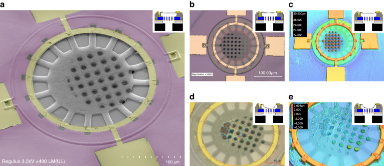
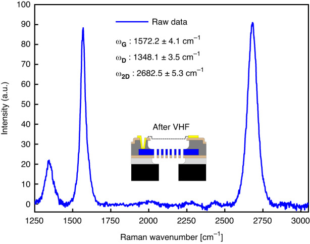
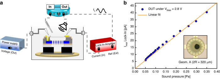
Since the performance of micro-electro-mechanical system (MEMS)-based microphones is approaching fundamental physical, design, and material limits, it has become challenging to improve them. Several works have demonstrated graphene's suitability as a microphone diaphragm. The potential for achieving smaller, more sensitive, and scalable on-chip MEMS microphones is yet to be determined. To address large graphene sizes, graphene-polymer heterostructures have been proposed, but they compromise performance due to added polymer mass and stiffness. This work demonstrates the first wafer-scale integrated MEMS condenser microphones with diameters of 2R = 220-320 μm, thickness of 7 nm multi-layer graphene, that is suspended over a back-plate with a residual gap of 5 μm. The microphones are manufactured with MEMS compatible wafer-scale technologies without any transfer steps or polymer layers that are more prone to contaminate and wrinkle the graphene. Different designs, all electrically integrated are fabricated and characterized allowing us to study the effects of the introduction of a back-plate for capacitive read-out. The devices show high mechanical compliances Cm = 0.081-1.07 μmPa-1 (10-100 × higher than the silicon reported in the state-of-the-art diaphragms) and pull-in voltages in the range of 2-9.5 V. In addition, to validate the proof of concept, we have electrically characterized the graphene microphone when subjected to sound actuation. An estimated sensitivity of S1kHz = 24.3-321 mV Pa-1 for a Vbias = 1.5 V was determined, which is 1.9-25.5 × higher than of state-of-the-art microphone devices while having a ~9 × smaller area.

Keywords: Electrical and electronic engineering; Engineering.


Conflict of interest statement

Competing interestsThe authors declare no competing interests.

Figures

Fig. 1
Fig. 1. Micromachining process flow.
The process steps to fabricate transfer-free multi-layer graphene condenser microphones are shown. (1) Definition of 1 μm SiO2 landing layer and 100 nm LPCVD SiNx etching mask for final back-side DRIE of the poly-Si venting holes. (2) LPCVD poly-Si (1 μm) and patterning, (3) PECVD TEOS (5 μm) and LPCVD SiNx (100 nm), (4) Dry-etching of SiNx for membrane area definition and vias for bottom-electrode contacts. (5) Mo sputtering (50 nm) and patterning, (6) CVD run for graphene growth, (7) Cr/Au 20/200 nm evaporation and lift-off, (8) Bosch process and SiO2 removal, (9) DRIE of poly-Si and (10) VHF of sacrificial layer
Fig. 2
Fig. 2. Device visualization by SEM and 3D laser scanning confocal microscope.
a SEM false color image of one final device (geom. C) in tilted view and low-magnification mode. Partial Cr/Au cracks are present on top of the multi-layer graphene tethers due to thermal stress experienced during the Cr/Au evaporation. A slower evaporation rate is found to improve the reported state. Undesired mask shift during the back-alignment step in hard contact resulted in misalignment and the unintended closure of venting holes. b Optical microscope image of the same device as in (a). c Laser topography image of the same device as in (a). d, e Optical microscope, and topography images of a collapsed device. As inset in (c, e), a height scale is added showing a downward deformation of the poly-Si back-plate due to thermal stress of ≈1.5% (center) of the suspended region. The main source of the compressive stress can be a residual thin layer of TEOS
Fig. 3
Fig. 3. Raman spectroscopy.
An example of material crystallinity at the end of the process after final release is shown in a wavenumber range of 1250–3000 cm−1. As an insight, all mean values and standard deviations are summarized. All acquisitions have been performed on the suspended multi-layer graphene in correspondence with the venting holes. Taking point in the free-standing area in correspondence with the back-plate leads to incorrect measurements due to suspended polysilicon influence on the backscattered signal
Fig. 4
Fig. 4. Membrane eigenfrequency.
First resonance frequency modes of the three different membranes are compared and fitted with Lorentz functions. The insets show stroboscopic topography data of the +z membrane displacement through the venting holes. Below, is a Comsol simulation of the mode-shapes of each of the geometries for different pre-tensions to match the experimental resonance frequencies
Fig. 5
Fig. 5. Base capacitance and pull-in.
a C0 – Vbias curves of the three geometries are compared with FEA results. The devices are driven with VAC = 100 mV and f1 = 100 kHz. b C0 – Vbias linear sweep from −9.5 V to 9.5 V describes the asymmetric membrane displacement of geom. b, d The blue numbers describe the membrane dynamics under Vbias increase of the inspected Geom. A device (also in Movie 2, Supp. mat. for geom. C). c Both electrodes are driven with a Vbias linear sweep from 0 V to 8 V. Despite the partial membrane collapse at Vbias = 3.8 V, no short circuits are found due to a residual TEOS thin layer (geom. A). d Membrane deflection under non-uniform electrostatic forces
Fig. 6
Fig. 6. Mechanical sensitivity at 1Pa in 10Hz - 10kHz.
In the legends are described the main parameters that have been used to fit the data with (Eq. (4)). The slope response for f > 10 Hz is mainly affected by n0 and the quality factor (Q). A better fitting for all proposed geometries in the slope for f > 800 Hz is found for low Q (overdamped systems) and original natural modes f01 values. The cut-off frequencies are 1500 Hz (Geom. A), 940 Hz (Geom. B), and 620 Hz (Geom. C)
Fig. 7
Fig. 7. Electrical response under sound actuation.
a The measurement setup employed for characterizing the device under test involves several components. The sample is secured to the chuck using double-sided tape covering the entire back side of the chip. Practical constraints drive this decision, as vacuum fixation is unfeasible within the experimental setup. Double-sided carbon tape serves the dual purpose of ensuring chip stability and ensuring that the sound pressure waves are only incident on the top side of the microphone. We note that this results in a relatively small back volume that increases the effective stiffness of the microphone compared to the configuration in Fig. 6. To bias the device, a power supply is utilized, which connects to the counter electrode. Simultaneously, a VAC driving signal from Moku:Lab (output) is employed to drive the speaker and serves as the external reference signal for the lock-in amplifier SR830. The membrane electrode is connected to the input of the lock-in amplifier in current mode. The LabVIEW script records the current output obtained from the lock-in amplifier. Additionally, the sound pressure is captured using a reference microphone connected to the Moku:Lab (input) positioned in close proximity to the device under test. b A trampoline with geom. A is driven by sound at f1 = 3 kHz at different pressure sound waves amplitudes p = 0.05–0.35 Pa. The Ip experimental curve is fitted with a linear fit

References

    1. Fueldner, M. In Handbook of Silicon Based MEMS Materials and Technologies 937–948 (Elsevier, 2020). 10.1016/b978-0-12-817786-0.00048-7.
    1. Shah MA, Shah IA, Lee D-G, Hur S. Design approaches of MEMS microphones for enhanced performance. J. Sens. 2019;2019:1–26. doi: 10.1155/2019/9294528. - DOI
    1. Zawawi SA, Hamzah AA, Majlis BY, Mohd-Yasin F. A review of MEMS capacitive microphones. Micromachines. 2020;11:484. doi: 10.3390/mi11050484. - DOI - PMC - PubMed
    1. Fu M, Dehe A, Lerch R. Analytical analysis and finite element simulation of advanced membranes for silicon microphones. IEEE Sens. J. 2005;5:857–863. doi: 10.1109/JSEN.2004.841449. - DOI
    1. Shubham S, et al. A novel MEMS capacitive microphone with semiconstrained diaphragm supported with center and peripheral backplate protrusions. Micromachines. 2021;13:22. doi: 10.3390/mi13010022. - DOI - PMC - PubMed