Review
. 2024 Feb 22;14(10):6656-6698.
doi: 10.1039/d4ra00433g. eCollection 2024 Feb 21.

Perovskite materials in X-ray detection and imaging: recent progress, challenges, and future prospects

Affiliations
Review

Perovskite materials in X-ray detection and imaging: recent progress, challenges, and future prospects

Md Helal Miah et al. RSC Adv. .

Abstract

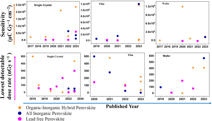
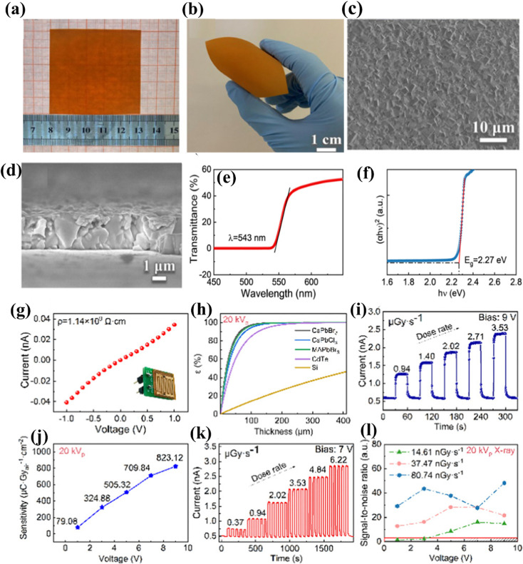
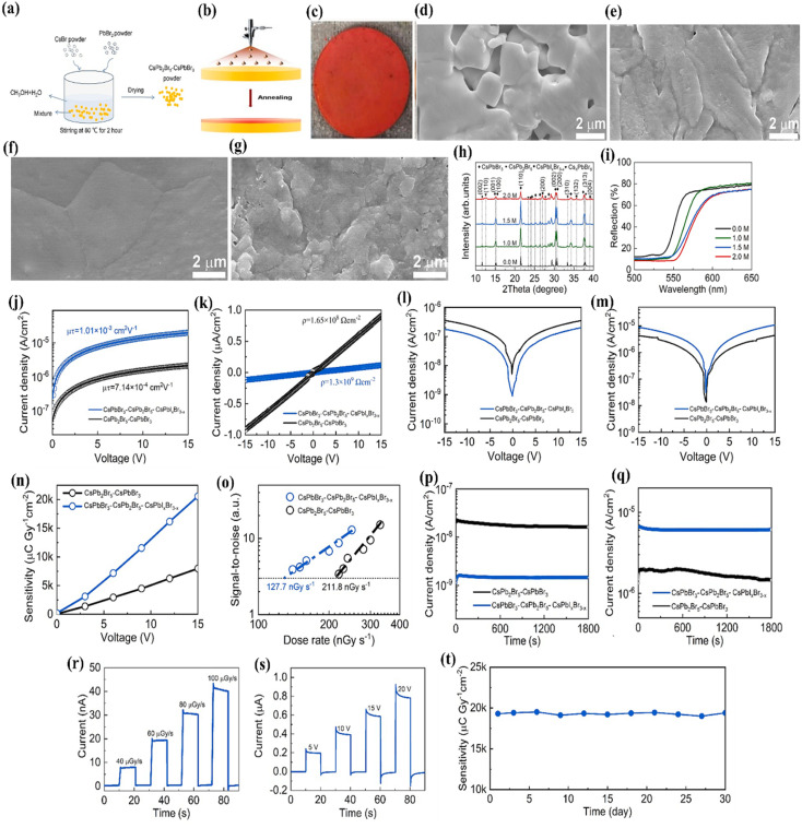
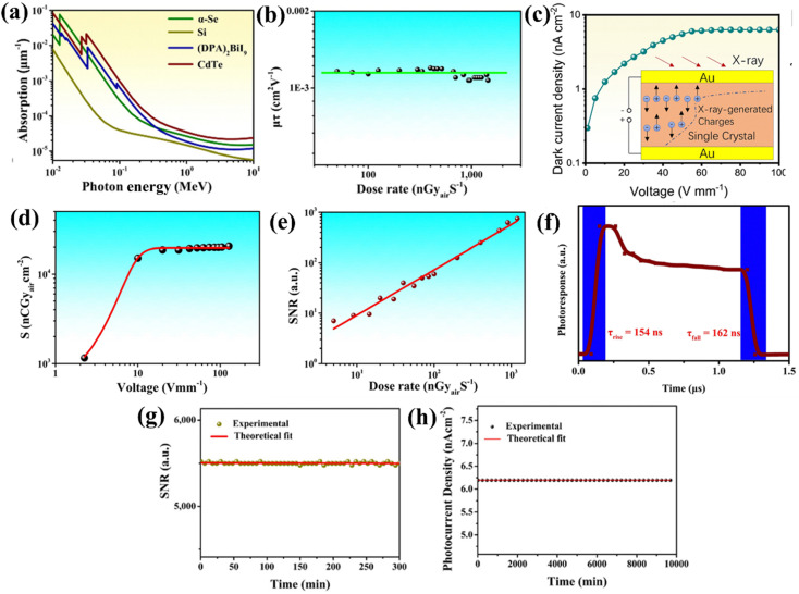
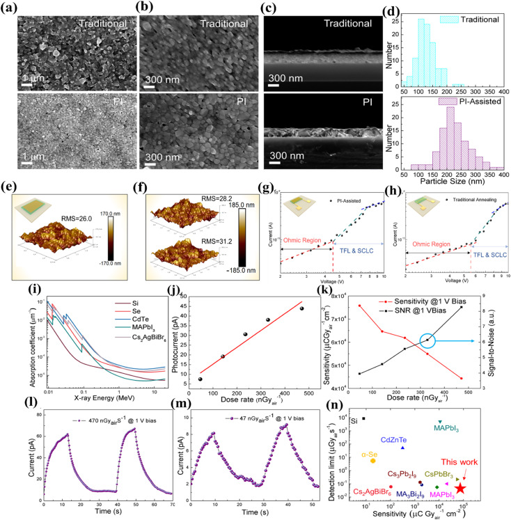
Perovskite materials have attracted significant attention as innovative and efficient X-ray detectors owing to their unique properties compared to traditional X-ray detectors. Herein, chronologically, we present an in-depth analysis of X-ray detection technologies employing organic-inorganic hybrids (OIHs), all-inorganic and lead-free perovskite material-based single crystals (SCs), thin/thick films and wafers. Particularly, this review systematically scrutinizes the advancement of the diverse synthesis methods, structural modifications, and device architectures exploited to enhance the radiation sensing performance. In addition, a critical analysis of the crucial factors affecting the performance of the devices is also provided. Our findings revealed that the improvement from single crystallization techniques dominated the film and wafer growth techniques. The probable reason for this is that SC-based devices display a lower trap density, higher resistivity, large carrier mobility and lifetime compared to film- and wafer-based devices. Ultimately, devices with SCs showed outstanding sensitivity and the lowest detectable dose rate (LDDR). These results are superior to some traditional X-ray detectors such as amorphous selenium and CZT. In addition, the limited performance of film-based devices is attributed to the defect formation in the bulk film, surfaces, and grain boundaries. However, wafer-based devices showed the worst performance because of the formation of voids, which impede the movement of charge carriers. We also observed that by performing structural modification, various research groups achieved high-performance devices together with stability. Finally, by fusing the findings from diverse research works, we provide a valuable resource for researchers in the field of X-ray detection, imaging and materials science. Ultimately, this review will serve as a roadmap for directing the difficulties associated with perovskite materials in X-ray detection and imaging, proposing insights into the recent status, challenges, and promising directions for future research.


Conflict of interest statement

The authors declare that they have no known competing financial interests or personal relationships that could have appeared to influence the work reported in this paper.

Figures

Fig. 1
Fig. 1. Working principle of a radiation detector.
Fig. 2
Fig. 2. Comparison of (a) atomic structure, (b) electronic behavior, (c) material characteristics, and (d and e) electrical properties of perovskite materials with different semiconducting materials for high-energy radiation detectors.
Fig. 3
Fig. 3. Brief essence of this review.
Fig. 4
Fig. 4. Some promising SC growth methods: (I) (a) temperature-dependent solubility of CsPbBr3 in DMSO and (b) inverse temperature crystallization. (II) (a) Temperature-dependent solubility of CsPbBr3 in water and (b) temperature-lowering crystallization. (III) Solvent evaporation method; (IV) anti-solvent vapor-assisted method; (V) hydrothermal method; and (VI) Bridgman method.
Fig. 5
Fig. 5. Various methods for developing films: (a) spin coating; (b) spray coating; (c) doctor blade coating; (d) inkjet printing method; and (e) ALS technique.
Fig. 6
Fig. 6. Isostatic-pressing method.
Fig. 7
Fig. 7. Sensitivity and lower detection dose rate (LDDR) of SC-, film- and wafer-based hybrid, all-inorganic and lead-free perovskite-based detectors.
Fig. 8
Fig. 8. (a–c) Continuous solution growth technique; (d–f) images of MAPbBr3 SCs; and (g) Idark curve for the device. (h) Current trace of the device across a bias range; (i) device current response to pulsed X-ray at various biases; (j) current response at various dose rates; (k) temporal photocurrent response for vertical surface detector; (l) schematic illustration of the imaging detector; (m) image of a hex nut on top of pixelated MAPbBr3 X-ray detector; and (n) X-ray image of the hex nut based on the ratio of photo-current (X-ray induced) to Idark. Reprinted with permission from ref. . Copyright 2023 Elsevier B.V.
Fig. 9
Fig. 9. (a) Cross-sectional SEM images of the Bi-doped MAPbI3 film; (b) cross-sectional SEM images of the p–n junction; (c) XRD outlining of the original p-MAPbI3 layer, and Bi-doped n-MAPbI3 layer; (d) dark I–V curves of the device with different Bi3+ concentrations; (e) X-ray (40 kV) sensitivity and Idark with respect to different Bi3+ concentrations at a biasing voltage 1 V; (f) absorption spectra of the n-MAPbI3 and p-MAPbI3 layers and curves of (αhν)2versus photon energy (inset); (g) snapshot of the bent X-ray detector (the bending radius is indicated by the red line in the circle); (h) sensitivity versus biasing voltage under illumination with a 40 kV X-ray source; (i) IV curves attained under different bending radii; (j) IT curves and (k) photo-current versus dose rate at 1 V under altering bending radii with respect to different dose rates; (l) sensitivity of the device under flat circumstances after 2000 bends with a 5 mm bending radius; (m) experimental X-ray imaging setup (schematic) during planar and curve X-ray imaging; (n) planar in top and curved in bottom X-ray imaging showing the “SEU” symbol; (o) real object of a ham with a nail and (p) X-ray images of a piece of ham with a nail inside. Reprinted with permission from ref. . Copyright 2023 @ The Royal Society of Chemistry.
Fig. 10
Fig. 10. (a) Schematic illustration of preparation of PbI2–DMSO-assisted isostatic pressing of MAPbI3 wafer; (b) SEM images (top view); (c) SEM images (cross-sectional); (d) AFM images; (e) photoconductivity; (f) resistivity; (g) JV characteristics; (h and i) PbI2–DMSO-assisted MAPbI3 device: current densities versus function of dose rate at different electric fields; (j) dose rate dependent SNR of the device; (k) photograph of a memory card and (l) X-ray image of the memory card. Reprinted with permission from ref. . Copyright 2023 @ Wiley Online Library.
Fig. 11
Fig. 11. (a) Schematic diagram of the vertical Bridgman furnace. (b) Photograph of an as-grown CsPbBr3 SCs. (c) XRD patterns of the (100), (010), and (001) facets of processed and polished wafers. (d–f) Photo-current fitting curves of the [100], [010], and [001] facets, respectively. (g) Photo-current response versus dose rates at −400 V. (h and i) X-ray sensitivities of the (100), (010), and (001) facet devices under various voltages. (j) Comparison of Idark drifts for the (100), (010), and (001) facet devices under a biasing voltage of −10 V. (k–m) Responses and SNR values dependent on the dose rate from 135 nGy s−1 to 260 nGy s−1 for the (100), (010), and (001) facet devices, respectively. (n) Detection limits (derived from the fitting line with an SNR of 3). Reprinted with permission from ref. . Copyright 2023@ The Royal Society of Chemistry.
Fig. 12
Fig. 12. Surface appearance of perovskite films with different thicknesses: (a) 400 nm, (b) 600 nm, and (c) 1000 nm CsPbI2Br on glass substrates and (d and e) AFM images in 10 μm scale for 400 nm and 600 nm, respectively. (f–k) X-ray detection by using the 1 μm CsPbI2Br device. (f) Current densities were measured in the dark and under AM 1.5 G conditions (voltage range of −2 V to 2 V). (g) Photo-current density versus time for X-ray dose rates in the range of 1.02 μGy s−1 to 12.59 μGy s−1. (h) Extracted photo-current densities produced from the respective dose rates. (i) SNRs estimated at dose rates in the range of 9.34 nGy s−1 to 74.75 nGy s−1. (j) Photo-current density versus time measured at 25.69 nGy s−1 dose rate (SNR = 3). (k) Normalized sensitivity of the device checked after 10 months. (l) Transient photo-current curve of the device measured by using a 635 nm pulsed diode laser (the light source). (m) Frequency response of the device. (n) Stability test of the device with illumination at a constant dose rate. (o) Battery box under closed and open conditions. (p) X-ray image of the object. Reprinted with permission from ref. . Copyright 2023@ the American Chemical Society.
Fig. 13
Fig. 13. (a and b) Photographs of a CsPbBr3 film; (c and d) top view and cross-sectional SEM images of the film; (e) UV-Vis-NIR transmission spectrum; (f) band gap of CsPbBr3 film fitted by a Tauc plot; (g) IV curves of the detector without and with X-ray at a biasing voltage of 1 V; (h) attenuation efficiency of various materials with a thickness in the range of 0–400 μm; (i) IT curves of the device under biasing 9 V irradiated by 20 kVp X-rays; (j) sensitivity of the device with respect to different voltages; (k) IT curves of the detector under a biasing voltage of 7 V and illuminated by X-rays of various dose rates; and (l) SNR of the CsPbBr3 detector under different biasing voltages and dose rates. Reprinted with permission from ref. . Copyright 2023 @ The Royal Society of Chemistry.
Fig. 14
Fig. 14. (a) Schematic technique for the fabrication of CsPbBr3–CsPb2Br5 powder by coprecipitation using H2O/methanol (MeOH) mixed solvent. (b) Schematic method for the preparation of CsPbBr3–CsPb2Br5–CsPbIxBr3−x wafer by spray coating by using CsI/H2O solution. (c) Image of CsPbBr3–CsPb2Br5–CsPbIxBr3−x composite wafers. (d–g) SEM images of CsPbBr3–CsPb2Br5–CsPbIxBr3−x wafers produced from (d) 0.0 M, (e) 1.0 M, (f) 1.5 M, and (g) 2.0 M CsI/H2O solution. (h) XRD patterns; (i) UV-Vis reflection spectra; (j) μτ product curves; (k) resistivity (ρ) versus voltage (V) curves; (l) JV curves recorded under the Idark condition; (m) JV curves with X-ray illumination; and (n) sensitivity plots for the CsPbBr3–CsPb2Br5 wafer and the CsPbBr3–CsPb2Br5–CsPbIxBr3−x composite wafer. (o) LDDR for the CsPbBr3–CsPb2Br5 wafer and CsPbBr3–CsPb2Br5–CsPbIxBr3−x wafer. (p and q) Current density versus time curves of X-ray detectors (p) without and (q) with X-ray irradiation; (r and s) current density versus time curves under different (r) radiation doses and (s) bias voltages for the detector and (t) long-term sensitivity test results. Reprinted with permission from ref. . Copyright@2023, Elsevier B.V. All rights reserved.
Fig. 15
Fig. 15. (a) Comparison of absorption coefficients of (DPA)2BiI9 with Si, CdTe and α-Se as photon energy functions and (b) μτ product of (DPA)2BiI9 along the c-axis. (c) Idark density versus voltage (inset: vertical structure of the X-ray device); (d) X-ray sensitivities versus voltage; (e) SNR value with respect to dose rates; (f) response time of the on and off states; (g) SNR value from stability test and (h) long-term X-ray photocurrent stability test. Reprinted with permission from ref. . Copyright 2023 @ The Royal Society of Chemistry.
Fig. 16
Fig. 16. (a and b) Top-view SEM images of Cs2AgBiBr6 films with different scales: films were fabricated via traditional annealing and PI tape-assisted annealing methods; (c) cross-sectional SEM images of the films; (d) statistics for the distribution of the perovskite crystal grain size with different annealing techniques; (e) AFM image of the PI-assisted film with the RMS (schematic diagram of annealing in inset); (f) comparison of AFM images prepared by PI-assisted techniques (upper) and conventional methods (lower) with their RMS; (g and h) IV relation of different films and the matching result (schematic illustration of the device in inset); (i) absorption coefficient for various X-ray energies of different materials; (j) current change with different dose rates of X-rays; (k) sensitivity and SNR of the PI-assisted film at different dose rates of X-rays; (l and m) IT response of the detector under 47 nGy s−1 and 470 nGy s−1, respectively; and (n) comparison of numerous X-ray detectors such as commercial ones and other perovskites. Reprinted with permission from ref. . Copyright 2023 @ the American Chemical Society.

Similar articles

Cited by

References

    1. Kasap S. O. Zahangir Kabir M. Rowlands J. A. Recent advances in X-ray photoconductors for direct conversion X-ray image detectors. Curr. Appl. Phys. 2006;6(3):288–292. doi: 10.1016/J.CAP.2005.11.001. - DOI
    1. Yang Y. Su Y. Ma W. Yang Y. M. Perovskite semiconductors for direct X-ray detection and imaging. J. Semicond. 2020;41(5):051204. doi: 10.1088/1674-4926/41/5/051204. - DOI
    1. Bernheim A. et al., Chest CT findings in coronavirus disease 2019 (COVID-19): Relationship to duration of infection. Radiology. 2020;295(3):685–691. doi: 10.1148/RADIOL.2020200463/ASSET/IMAGES/LARGE/RADIOL.2020200463.FIG5B.JPEG. - DOI - PMC - PubMed
    1. Hu H. Shen L. Guan Q. Li X. Zhou Q. Ruan S. Deep co-supervision and attention fusion strategy for automatic COVID-19 lung infection segmentation on CT images. Pattern Recognit. 2022;124:108452. doi: 10.1016/J.PATCOG.2021.108452. - DOI - PMC - PubMed
    1. Zhang F. Y. Qiao Y. Zhang H. CT imaging of the COVID-19. J. Formosan Med. Assoc. 2020;119(5):990–992. doi: 10.1016/J.JFMA.2020.04.006. - DOI - PMC - PubMed