Review
. 2024 Mar 4;15(1):1974.
doi: 10.1038/s41467-024-45670-9.

Hardware implementation of memristor-based artificial neural networks

Affiliations
Review

Hardware implementation of memristor-based artificial neural networks

Fernando Aguirre et al. Nat Commun. .

Abstract

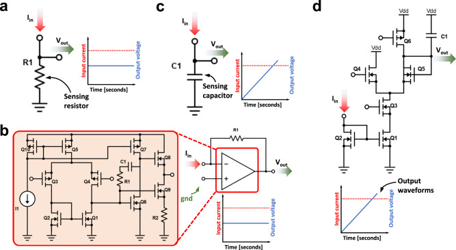
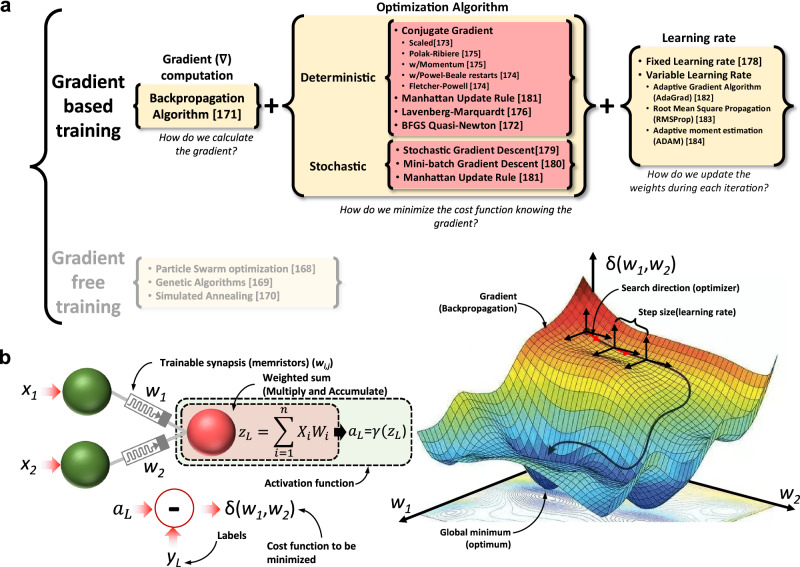
Artificial Intelligence (AI) is currently experiencing a bloom driven by deep learning (DL) techniques, which rely on networks of connected simple computing units operating in parallel. The low communication bandwidth between memory and processing units in conventional von Neumann machines does not support the requirements of emerging applications that rely extensively on large sets of data. More recent computing paradigms, such as high parallelization and near-memory computing, help alleviate the data communication bottleneck to some extent, but paradigm- shifting concepts are required. Memristors, a novel beyond-complementary metal-oxide-semiconductor (CMOS) technology, are a promising choice for memory devices due to their unique intrinsic device-level properties, enabling both storing and computing with a small, massively-parallel footprint at low power. Theoretically, this directly translates to a major boost in energy efficiency and computational throughput, but various practical challenges remain. In this work we review the latest efforts for achieving hardware-based memristive artificial neural networks (ANNs), describing with detail the working principia of each block and the different design alternatives with their own advantages and disadvantages, as well as the tools required for accurate estimation of performance metrics. Ultimately, we aim to provide a comprehensive protocol of the materials and methods involved in memristive neural networks to those aiming to start working in this field and the experts looking for a holistic approach.


Conflict of interest statement

The authors declare no competing interests.

Figures

Fig. 1
Fig. 1. Computing power demand increase and platform transition from Von-Neumann towards highly parallelized architectures.
a The increase in computing power demands over the past four decades expressed in petaFLOPS per days. Until 2012, computing power demand doubled every 24 months; recently this has shortened to approximately every 2 months. The colour legend indicates different application domains. Mehonic, A., Kenyon, A.J. Brain-inspired computing needs a master plan. Nature 604, 255–260 (2022), reproduced with permission from SNCSC. b A comparison of neural network accelerators for FPGA, ASIC, and GPU devices in terms of speed and power consumption. GOP/s giga operations per second, TOP/s tera operations per second.
Fig. 2
Fig. 2. Generalized block diagram indicating the required circuital blocks to implement a memristive ANN for pattern classification.
Green blocks (3, 5, 7 and 8) indicate the required mathematical operations (such as the VMM or activation functions). Red blocks (1, 2, 4, 6, 9, 11, 12, 13, 14, 15, 16) identify the required circuits for signal adaptation and/or conversion. The data path followed during the inference (or forward pass) is indicated by the red arrows/lines. The data path followed for in-situ training is indicated by the blue arrows/lines. The data path followed under ex-situ training is shown by the yellow arrows/lines. For each box, the upper (colored) part indicates the name of the function to realize by the circuital block, and the bottom part indicates the type of hardware required. The box titled successive neural layers would encompass multiple sub-blocks with a structure similar to the group titled First neural layer. 1S1R stands for 1Selector 1 Resistor while 1R stands for 1 Resistor. UART, SPI and I2C are well known communication standards. RISC stands for Reduced Instruction Set Computer.
Fig. 3
Fig. 3. Non-Von Neumann vector-matrix-multiplication (VMM) cores reported in the literature.
a Full-CMOS SRAM (Static Random Access Memory) crossbar array, b Hybrid memristor/CMOS 1T1R crossbar array and c Full-memristive passive crossbar array. All cases assume a crossbar array integration structure which performs the Multiply-and-Accumulate (MAC) by exploiting the Kirchhoff’s law of currents. The use of memristors allows a smaller footprint per synapse as a lower number of smaller devices is employed. Passive crossbar arrays of memristors allow the highest possible integration density, yet they are still an immature technology with plenty of room for optimization. a Yamaoka, M. Low-Power SRAM. In: Kawahara, T., Mizuno, H. (eds) Green Computing with Emerging Memory. Springer, New York, NY (2013), reproduced with permission from SNCSC. b is adapted with permission under CC BY 4.0 license from ref. . c is adapted with permission under CC BY 4.0 license from ref. . F is the feature size of the litography and the energy estimation is on the cell-level. FEOL and BEOL stands for Front End Of Line and Back End Of Line, respectively.
Fig. 4
Fig. 4. Example of a widely popular image database used for ANNs training and test, and how they are feed to the network.
a Samples of the MNIST dataset of handwritten numeric digits considered in this article. In all cases images are represented in 28 × 28 px. Pixel brightness (or intensity) is codified in 256 levels ranging from 0 (fully OFF, black) to 1 (fully ON, white). b Readability loss as the resolution decreases from 28 × 28 pixels (case I) to 8 × 8 (case IV). c Schematic representation of the unrolling of the image pixels. Note that each of the n image columns of pixels are vertically concatenated to reach a n2 × 1 column vector. It is then scaled by VREAD to produce a vector of analogue voltages that is fed to the ANN.
Fig. 5
Fig. 5. Schematic diagrams of DAC circuits conventionally used in the literature to bias the rows of the memristive crossbar.
a N-bit weighted Binary, b Current-steering DAC, c Memristive-DAC d N-bit R-2R DAC and e Pulse Width Modulation (PWM)-based DAC.
Fig. 6
Fig. 6. Memristor crossbar structure and electrical connection diagram for signed weights representation.
a Sketch of the crossbar array structure. Red and blue arrows exemplify the electron flow through the memristors connecting the top (Word lines -WL-) and bottom lines (Bit lines -BL-). Different memristor resistance states are schematically represented (High Resistance State -HRS- to Low Resistance State -LRS-). The dashed blue line depicts the so-called sneak path problem. The parasitic wire resistance is indicated for WLi and BLi. Reproduced with permission under CCBY 4.0 license from ref. . b Equivalent circuit representation of the CPA sketched in a, showing the input voltages, output currents and TIA blocks that translates the output CPA current to a vector of analogue voltages. In this case the circuit was simplified by ignoring the line resistances. Finally, two different realizations of the memristive-based ANN synaptic layer are shown in c – unbalanced – and d – balanced –.
Fig. 7
Fig. 7. Circuit schematics for the sensing electronics placed in at the output of every column of the memristive crossbar.
In all cases, the goal is to translate a current signal into a voltage signal. a The sensing resistor is the simplest case, as it translates current into voltage directly by the Ohm’s law. b The use of a TIA allows to connect the crossbar columns to 0 volts and operate with lower output currents. As well as in the resistor-based approach, the current voltage conversion is linear when operating the TIA within its linear range and the output voltage signal is immediately available as soon as the output of the TIA settles. c For currents below the nano-ampere regime, charge integration is the most suitable option for current-voltage conversion. This can be achieved by using a capacitor. As such, the measurement is not instantaneous as a constant, controllable integration time is required before the measurement. d To minimize the area requirements of the integration capacitor, the use of a current divider allows to further reduce the current and, with it, the size of the required capacitor. The tradeoff in this case is with precision (mainly due to transistor mismatch) and output voltage dynamic range.
Fig. 8
Fig. 8. Equivalent electrical circuit of the topology used to implement the mathematical difference between two electrical signals.
a Assuming that voltage inputs are unipolar (that is, only negative or positive), it is required to first transduce the current signals into voltage and then add an operational amplifier in a subtractor configuration. b If bipolar signals can be applied in the inputs, by biasing the negative synaptic weights with a voltage or opposite polarity, summing the resulting currents in a common node (Kirchhoff’s Law for Current) already solves the subtraction operation, and only one transimpedance amplifier is required per column.
Fig. 9
Fig. 9. Circuital implementations of the analogue activation functions used in memristive neural networks.
Full-CMOS implementations of the a sigmoid and b ReLU activation functions. Aiming to minimize the area footprint of the activation function, c presents a ReLU implementation based on a VO2 Mott insulator device.
Fig. 10
Fig. 10. Analogue CMOS implementation of the Winner-Takes-All (WTA) function.
a WTA CMOS block with voltage input. The gate terminal of transistor Q5, and the source terminals of transistors Q6 and Q7 are common to all WTA cells. b WTA CMOS block with current input. Node Vcom is common to all WTA cells. In both cases, the output voltage of the WTA cell with the highest input voltage/current is driven to the positive reference voltage (VDD), while the output voltage of the remaining WTA cells is driven to ground. The number of cells in the WTA module is the same to the number of classes of images to identify by the ANN.
Fig. 11
Fig. 11. Schematic diagrams of ADC circuits conventionally used in the literature.
a SAR-ADC, b ΔΣ-ADC, c CCO-ADC, d VCO-based ADC and e Flash ADC.
Fig. 12
Fig. 12. Basic concepts of neural network training.
a Simplified organization of the most common terms reported in the literature, differentiating between gradient based and gradient free training tools. For the gradient-based tools, we propose an organization of the algorithms for (i) gradient computation, (ii) optimization and (iii) learning rate. b Illustration of the gradient descent method, for a trivial 2 × 1 neural network trained with supervised learning.
Fig. 13
Fig. 13. k-fold cross validation with 10 repeats considering 11 different learning algorithms.
,– The accuracy obtained in each repeat is plotted against the CPU run-time of the learning algorithm when trained for the MNIST dataset for two different resolutions: a 8 × 8 and b 28 × 28 px. images. Although the Levenberg-Marquardt algorithm shows the higher mean accuracy, it is also the slowest to converge in our implementation, especially when considering large-size networks, as those required for classifying the 28 × 28 px. images. As a trade-off between accuracy and learning time, we have considered for the example to be described in later in this article, the Scaled Conjugate Gradient, as the accuracy difference with the Levenberg-Marquardt method is not statistically relevant: i.e., the observed difference might be due to a data fluctuation in the test dataset.
Fig. 14
Fig. 14. Typical figures-of-merit used to quantify the performance of ANNs intended for pattern recognition.
In this case, they are plotted as a function of the training epochs. a Accuracy, b confusion matrix, c Loss function (cross-entropy), d Sensitivity, e Specificity, f Precision, g F1-score, h κ-coefficient.
Fig. 15
Fig. 15. Schematic representation of the trade-off between simulation speed and accuracy across the different tools reported in the literature for memristive ANNs evaluation.
For each case, we list the main programming languages involved and some examples.
Fig. 16
Fig. 16. Detail of the different stages of the transaction level modelling, with the addition of the Neural Network and transistor (circuit) level simulation.
Modelling approaches are arranged based on how accurately (untimed, approximate, cycle-accurate) the timing of the computation and communication aspects are captured. Transaction level models then expand from B to G, with B being the specification models (which uses considers the communication and computation to be untimed) and G the implementation models (which considers both cycle-accurate timing for both computation and communication). As we approach B, the model can be regarded as a System Level Simulation, while if it approaches G, it is regarded as an architecture-level simulation. Outside this group, we find those models simulated in Python or similar tools which focus on the network topology (A) and the circuital models which materializes the implementation models (G) in the transistor or register transfer level.
Fig. 17
Fig. 17. Different representations of the Vector Matrix Multiplication operation typical from a synaptic layer.
(a) Unitless mathematic VMM operation. (b) Mathematic VMM operation involving electrical magnitudes. (c) Electrical circuit representation of the memristive crossbar-based analogue VMM operation. (d) Realistic memristor crossbar representation considering the line resistance (RL) and the interline capacitances (see the inset showing a circuit schematic of a memristive cell in a CPA structure considering the associated wire parasitic resistance and capacitance). Aspects such as device variability are captured by the memristor model employed.
Fig. 18
Fig. 18. Connections schemes used to feed the CPA with the input pattern.
a Single Side Connect (SSC) and (b) Dual Side Connect (DSC). On the SSC case, the input stimuli are applied only to the inputs of one side of the CPA, while the other is connected to high impedances (or remain disconnected). b In the DSC case, both terminals of a given wordline (horizontal lines in the CPA) are connected to the same input voltage, which thereby reduces the voltage drop along the wordlines.
Fig. 19
Fig. 19. Detail of the control circuits used for the dual inference/write procedures.
a complete circuit schematic for a 4×8 1T1R crossbar array. b Detail of the synchronizers including the sense amplifiers used to detect the correct programming of a given memristor. c Address block, essentially a counter which sequentially addresses each memristor in the crossbar. d Row and column decoders, used to enable the memristor addressed by the address block. e Row and column driver, used to bias the rows with the voltage input or with the programming signal, and to connect the columns to the output neurons (during inference) or the sense amplifier (during write-verify).
Fig. 20
Fig. 20. Schematic representation of the n2×1 column vectors of analogue voltages being fed to the SLP.
4 cases are represented: ac corresponds to the correct classification of images from classes k, k+1 and k-1, respectively (for instance, in the case of the MNIST database, they might be images of the ‘5’, ‘6’ and ‘4’ digits). d Depicts the case of misclassification, as the highest current corresponds to the k+1 output for an image from class k.
Fig. 21
Fig. 21. Write-verify approach for conductance programming.
a Schematic representation of the Write-Verify loop approach for programming the memristors in the CPA to a given conductance value. Reproduced with permission under CCBY 4.0 license from ref. . b Sensed output current for a SLP partition (one small CPA) during the programming phase in a Write-Verify loop procedure. The greater the peak, the higher the conductance level being programmed. The inset in the center shows a schematic representation of the current measured during the verify and write pulses, as well as the current target. The inset in the right of both panels shows a schematic of the equivalent circuit using during the verify phase. Reproduced with permission under CCBY 4.0 license from ref. .

Similar articles

Cited by

References

    1. European Commission, Harnessing the economic benefits of Artificial Intelligence. Digital Transformation Monitor, no. November, 8, 2017.
    1. Rattani, A. Reddy, N. and Derakhshani, R. “Multi-biometric Convolutional Neural Networks for Mobile User Authentication,” 2018 IEEE International Symposium on Technologies for Homeland Security, HST 2018, 10.1109/THS.2018.8574173 2018.
    1. BBVA, Biometrics and machine learning: the accurate, secure way to access your bank Accessed: Jan. 21, 2024. [Online]. Available: https://www.bbva.com/en/biometrics-and-machine-learning-the-accurate-sec...
    1. Amerini I, Li C-T, Caldelli R. Social network identification through image classification with CNN. IEEE Access. 2019;7:35264–35273. doi: 10.1109/ACCESS.2019.2903876. - DOI
    1. Ingle P. Y. and Kim, Y. G. “Real-time abnormal object detection for video surveillance in smart cities,” Sensors, 22,10.3390/s22103862 2022. - PMC - PubMed