. 2024 Mar 7;14(1):5626.
doi: 10.1038/s41598-024-55255-7.

An analytical approach to engineer multistability in the oscillatory response of a pulse-driven ReRAM

Affiliations

An analytical approach to engineer multistability in the oscillatory response of a pulse-driven ReRAM

Alon Ascoli et al. Sci Rep. .

Erratum in

Abstract

A nonlinear system, exhibiting a unique asymptotic behaviour, while being continuously subject to a stimulus from a certain class, is said to suffer from fading memory. This interesting phenomenon was first uncovered in a non-volatile tantalum oxide-based memristor from Hewlett Packard Labs back in 2016 out of a deep numerical investigation of a predictive mathematical description, known as the Strachan model, later corroborated by experimental validation. It was then found out that fading memory is ubiquitous in non-volatile resistance switching memories. A nonlinear system may however also exhibit a local form of fading memory, in case, under an excitation from a given family, it may approach one of a number of distinct attractors, depending upon the initial condition. A recent bifurcation study of the Strachan model revealed how, under specific train stimuli, composed of two square pulses of opposite polarity per cycle, the simplest form of local fading memory affects the transient dynamics of the aforementioned Resistive Random Access Memory cell, which, would asymptotically act as a bistable oscillator. In this manuscript we propose an analytical methodology, based on the application of analysis tools from Nonlinear System Theory to the Strachan model, to craft the properties of a generalised pulse train stimulus in such a way to induce the emergence of complex local fading memory effects in the nano-device, which would consequently display an interesting tuneable multistable oscillatory response, around desired resistance states. The last part of the manuscript discusses a case study, shedding light on a potential application of the local history erase effects, induced in the device via pulse train stimulation, for compensating the unwanted yet unavoidable drifts in its resistance state under power off conditions.

Keywords: Fading memory; Local fading memory; Multistability; Nonvolatility; ReRAM.


Conflict of interest statement

The authors declare no competing interests.

Figures

Figure 1
Figure 1
(a) Circuit employed to investigate the response of the Ta2O5-x ReRAM cell to periodic square pulse-based voltage excitation signals. (b) Time course of a two-pulse-per-cycle train voltage stimulus. (c) Time waveform of a generalised pulse train voltage stimulus vS, including P positive SET pulses and one negative RESET pulse per cycle. The RESET pulse of height V- and width τ- follows the series of SET pulses. The ith SET pulse is V+,i high and τ+,i wide, with i{1,,P}. The ordering of the positive pulses from the lowest to the highest in each input cycle follows the convention adopted in the systematic methodology to engineer multistability in the steady-state oscillatory response of the ReRAM cell to a generalised train stimulus (refer to section “A systematic methodology to craft the pulse stimulus for enabling the ReRAM cell to support multiple oscillations around prescribed resistance levels”. However, this has no effect on the simulations. In fact, to facilitate their convergence, in the numerical investigations, discussed in section “Conclusions”, the SET pulses were listed from the most narrow to the most wide before being applied in this order one after the other across the device.
Figure 2
Figure 2
(a) Blue (Red) trace: SET x¯˙SET (RESET x¯˙RESET) component of the TA-SE (10) of the ReRAM cell under an arbitrary pulse train stimulation. (b) Moduli of the SET and RESET TA-SE components. Their intersections identify the TA-SE equilibria. (c) TA-SDR of the ReRAM cell subject to the arbitrarily chosen pulse train stimulus. Arrows, pointing to the east (west), are superimposed along any TA-SDR branch, which visits the upper (lower) half plane, so as to indicate a progressive increase (decrease) in the time average state x¯ when x¯˙ is positive (negative). An equilibrium for the TA-SE exists at the abscissa x¯=x¯eq of any point, at which the TA-SDR crosses the horizontal axis, as x¯˙=0 therein. The equilibrium is asymptotically stable (unstable), as indicated via a black filled (red hollow) circle, if and only if the slope x¯˙/x¯ of the x¯˙ versus x¯ locus is negative (positive) at its location. According to the TA-SDR analysis, the ReRAM cell is expected to act as a bistable oscillator under the given periodic excitation.
Figure 3
Figure 3
(a) Exemplary illustration of a one-dimensional discrete-time system xk=P(xk-1), referred to as Poincaré map, which admits three intersections with the identity map xk=PI(xk-1)=xk-1, representing its fixed points, specifically x1, x2, and x3, of which the outer ones (inner one) are stable (is unstable). A few coloured zig-zag trajectories, known as cob-web plots, in Nonlinear Dynamics Theory, are also displayed to show the discrete-time evolution of the map from distinct initial conditions toward one of the two LAS fixed points. In our study a map of this kind can be extracted from the Strachan DAE set, when the input voltage v is enforced to follow a given periodic voltage stimulus vS, e.g. in the form of a rectangular pulse train, by recording samples of the memristor state x at regular T-long time intervals from the beginning of each of a large ensemble of simulations, differing in the initial conditions, and then plotting for each of the resulting time series the kth sample xk=x(k·T) versus the (k-1)th one xk-1=x((k-1)·T), with kN>0. For k=1 the SCPCM reduces to Δ1;0=x1-x0=P(x0)-x0, providing the change in the memory state over the first input cycle. (b) Δxk;k-1=xk-xk-1 versus xk-1 locus, illustrating the SCPCM of the ReRAM cell subject to the periodic stimulus, which induces a state motion resulting in the Poincaré map shown in plot (a).
Figure 4
Figure 4
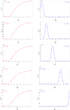
(a), (c), (e), (g), (i) ((b), (d), (f), (h), (l)) gRESET(x,V) (gSET(x,V)) versus x locus, denoting the RESET (SET) SDR of the ReRAM cell when V is chosen as the first, second, third, fourth, and fifth value from the set {-(+)0.2,-(+)0.4,-(+)0.6,-(+)0.8,-(+)1}V. Over a RESET (SET) resistance switching transition the device state undergoes a progressive decrease (increase), as the arrows, superimposed on top of the respective SDR, clearly indicate through their westward (eastward) direction. With reference to each graph along the first column, the red filled circle shows the location of the stable equilibrium xeq=xL, which the ODE (1) admits for any negative bias value V assigned to the input voltage v. On the other hand, the state equation admits no equilibrium under any positive DC stimulus.
Figure 5
Figure 5
Three-dimensional illustration, showing each admissible stable or unstable equilibrium x¯eq=x¯eq(V+,V-), which the TA-SE (10), associated to a train voltage stimulus, featuring two pulses of opposite polarity per cycle, may possibly admit, when the SET τ+ and RESET τ- pulse widths are identical, as a function of the SET V+ and RESET V- pulse heights, swept across the ranges [-2,0]V and [0,1.2]V, respectively. The dark blue surface includes all the GAS equilibria of the TA-SE in the monostable oscillatory operating mode of the ReRAM cell. The cyan (magenta) surface contains all the unstable (all the LAS) equilibria of the TA-SE in the bistable oscillatory operating mode of the ReRAM cell. (b) Projection of the surface from (a) onto the V+ versus V- plane. Choosing the pulses’ heights of the pulse train voltage stimulus, featuring a 50% duty cycle, according to the coordinates of any point in the green (red) region, the TA-SE features a single GAS equilibrium (two LAS equilibria) for r=1. The black cross marker (black plus sign) identifies the input parameter pair (V-,V+), inducing the particular monostable (bistable) oscillatory response, illustrated in Fig. 6 (Fig. 7), in the nanodevice.
Figure 6
Figure 6
SET |x¯˙SET| (blue trace) and RESET |x¯˙RESET| (red trace) components of the TA-SDR of the ReRAM cell under the application of a two-pulse-per-cycle pulse train voltage stimulus vS, when its SET V+ and RESET V- pulse heights are in turn set to +0.46V and -0.4V, and for r=1, irrespective of the choice of its SET τ+ and RESET τ- pulse widths. Note that scaling the widths of the 2 pulses in the train per cycle by the same factor does not affect the TA-SDR prediction. The only GAS equilibrium x¯eq of the TA-SE lies at 0.308, which is the abscissa of the black-filled circle. A marker, indicating the zero of the RESET component at x¯=0, is omitted from the graph, so as to avoid clutter. (b) SCPCM of the ReRAM cell subject to a particular pulse train voltage stimulus vS, belonging to the class considered in (a), and characterised by parameters (V+,τ+,V-,τ-)=(+0.46V,1μs,-0.4V,1μs) (refer to the blue signal of period T=τ++τ-=2μs in plot (d)). The Poincaré map, from which it is extracted, features a GAS fixed point x (see the black-filled circle). Differently from what is the case for the TA-SDR, scaling the widths of the 2 pulses in the train per cycle by the same factor may affect the SCPCM. (c) Brown (Green) trace: progressive approach of the solution x to the Strachan DAE set, when v is forced to follow the particular excitation voltage signal vS, employed for the derivation of the SCPCM, from the initial condition x0=x0,1=0.15 (x0=x0,2=0.85) toward a unique steady-state oscillation. (d) Green trace: steady-state time series xss of the memristor state x, as extracted from the solution featuring the same colour in plot (c). Horizontal lines mark the locations of the map fixed point x, of the TA-SE equilibrium x¯eq, and of the time average x¯ss of the steady-state time series. As the RESET pulse follows the SET pulse over each cycle of the input train, xss attains its minimum value at the end of any period. Therefore x directly reveals the minimum of xss across one input cycle.
Figure 7
Figure 7
Decomposition of the TA-SDR into its SET |x¯˙SET| (blue trace) and RESET |x¯˙RESET| (red trace) components—plot (a)—for the ReRAM cell subject to a two pulse-per-cycle pulse train voltage stimulus vS, composed of one SET (RESET) pulse of positive (negative) amplitude V+=+0.54V (V-=-0.6V) over the first (second) τ+(τ-)-long half of each period of duration T=τ++τ-, irrespective of the common value assigned to τ+ and τ-. The TA-SE admits a triplet of equilibria, namely x¯eq,1=0.106, x¯eq,2=0.237, and x¯eq,3=0.370. Each of the outer ones (The inner one), indicated via a black-filled (red hollow) circle, is LAS (unstable). (b) Time waveform of a particular pulse train voltage stimulus, belonging to the class assumed in (a), and identified via the parameter quartet (V+,τ+,V-,τ-)=(+0.54V,20ps,-0.6V,20ps). (c) SCPCM of the ReRAM cell in the case, where the excitation voltage signal vS from (b) is let fall continuously between its terminals. A black-filled (red hollow) circle denotes a locally-stable (an unstable) fixed point for the associated Poincaré map. (d) Cyan (Violet) trace: time course of the memory state x of the ReRAM cell, with voltage v forced to follow vS from (b) at all times, from the initial condition x=x0,1=0.2 (x=x0,2=0.3). Unlike the latter solution, the first one takes a very long time to attain the steady state. (e, f) Locally-stable oscillatory solution x1 (x3) for the state x of the ReRAM cell, as recorded in a numerical simulation of the Strachan DAE set under v=vS from (b) for x0=x1 (x0=x3). In each of the two cases the choice of the initial condition ensures that no transients appear in the device response. The time average x¯1 (x¯3) of the solution x1 (x3), as well as the corresponding LAS TA-SE equilibrium x¯eq,1 (x¯eq,3) and LAS map fixed point x1 (x3) are also marked in plot (e, f).
Figure 8
Figure 8
(a) Coloured map, depicting how the number of admissible stable or unstable equilibria for the TA-SE of the ReRAM cell, subject to a two-pulse-per-cycle pulse train voltage stimulus from the class illustrated in Fig. 1b is influenced by the SET pulse amplitude V+ as well as by the ratio r between the SET and RESET pulse widths, given a RESET pulse amplitude V- of -0.5V. The green and red regions respectively enclose input parameter pairs, which endow the TA-SE with one and only one GAS equilibrium (three equilibria, of which the outer ones are LAS). (b, c) Graphical illustration, showing the decomposition of the TA-SDR into its SET and RESET components for a scenario, where the input pair (V+,r), lying at (+0.50V,1×108) ((+0.75V,1×10-30)) (see the black cross marker (black plus sign) within the green (red) region of the map in (a)), determines the existence of one and only one GAS equilibrium x¯eq=0.314 (three equilibria x¯eq,1=0.042, x¯eq,2=0.516, and x¯eq,3=0.725, of which the outer ones are LAS) for the respective TA-SE.
Figure 9
Figure 9
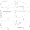
(a) Dependence of the abscissa xmax of the peak of the gaussian bell, illustrating a SET SDR, i.e. a gSET(x,V) versus x locus from the ReRAM cell DRM (refer for examples to plots (b), (d), (f), (h), and (l) of Fig. 4), upon the positive DC voltage V=V+[0,1]V. The exact analytical solution, descending from the formula (17), is illustrated in red. The numerical solution, depicted in blue, saturates abruptly to the unitary value at the first positive DC voltage V+, specifically 0.957V, where xmax exceeds the upper bound xU of the state existence domain D, keeping unchanged for any larger V+ value. (b) Blue trace: Graph of γ as a function of V+, according to the exact analytical formula (18). Red trace: approximation of the γ versus V+ locus via the analytical function γ~(V+,V+,1,V+,2) from Eq. (19) for (V+,1,V+,2)=(V+,1(opt),V+,2(opt))=(0.662,0.923)V. (c) Positive value V+ to be assigned to the DC voltage V in order for the abscissa of the peak of the resulting SET SDR to lie at a pre-specified location xmax. The blue curve shows the V+ versus xmax locus determined numerically from the blue-coloured numerical solution in (a) by exchanging the data series reported along horizontal and vertical axes. At xmax=1 the blue trace abruptly turns into a vertical segment stretching from V+=0.957V to V+=1V. The red curve is the V~+ versus xmax locus, extracted from the analytical formula (22), proposed to approximate the inverse of the function (17), for V+,1=V+,1(opt), and V+,2=V+,2(opt). (d) Blue trace: graphical illustration of the exact analytical formula (17) for xmax. Red trace: x~max versus V+ locus, obtained from the approximate closed-form expression (20) for (V+,1,V+,2)=(V+,1(opt),V+,2(opt)). (e) Peak value gSET, max(V+) of a SET SDR as a function of the positive DC voltage V+ across the ReRAM cell. The red trace shows the exact analytical solution, derived from the closed-form expression (27), while the blue trace depicts its numerical counterpart. (f) Impact of the positive DC voltage V+ on the width wk(V+) of the respective SET SDR, measured as the distance between the state values x+,k and x-,k, at which gSET(x,V+) appears to be scaled down by a factor k as compared to its peak value gSET(xmax,V+), for each k value from the set {1.5,2,3}. The exact analytical solution, descending from the formula (35), (The numerical solution) is illustrated through a dashed (solid) trace with red (blue), magenta (black), and green (brown) hue for the first, second, and third k value from the triplet. When 1.5, 2, and 3 is assigned to k, the numerical solution deviates from the corresponding analytical one as soon as V descends below +0.184, +0.211, +0.237V (increases above +0.937, +0.932, and +0.925V), since then x- (x+) descends below (rises above) the lower (upper) bound xL (xU) in the state existence domain D.
Figure 10
Figure 10
Surface of the maximum squared error maxxmaxD{e2(xmax,V+,1,V+,2)} as a function of the voltage parameters V+,1 and V+,2 under optimisation. At each of the points (V+,1,V+,2)=(0.662,0.923)V and (V+,1,V+,2)=(0.923,0.662)V, marked as red circles, and symmetrically located relative to the plane V+,2=V+,1, the surface assumes the minimum possible value, specifically 5.635×10⁻⁸. Without loss of generality, in the remainder of this paper V+,2 is assumed to be larger than V+,1. As a result the optimal parameter pair is chosen as (V+,1(opt),V+,2(opt))=(0.662,0.923)V.
Figure 11
Figure 11
Illustrations elucidating how to choose the design parameter k for a case study, where it is requested for the ReRAM cell to act as a bistable oscillator under the application of a three-pulse-per-cycle pulse train voltage stimulus between its terminals. Let the ith positive pulse in the input sequence over each cycle have amplitude V+,i and width τ+,i, for i{1,2}. The negative pulse, following the two positive ones in each input cycle, is assumed to feature a fixed amplitude V- of -0.5V, while its width τ- is to be determined. It is further required for the left LAS TA-SE equilibrium x¯eq,1 to be located at 0.280. The right LAS TA-SE equilibrium x¯eq,3 should be apart from the left one by one bell width wk. When k is set to 1.5, 2, and 3, x¯eq,3 is expected to lie at 0.356, 0.380, and 0.406, respectively. (a) For k=1.5 the application of the design methodology first employs the approximate analytical formula (22), with xmax set to xmax,1=x¯eq,1-w1.5/4 (xmax,2=x¯eq,3-w1.5/4), V+,1=V+,1(opt), and V+,2=V+,2(opt), to fix the amplitude V+,1 (V+,2) of the first (second) SET pulse to 0.483V (0.550V). It then specifies the values 0.815 and 2.687×10⁻⁵ for r+,1 and r+,2, respectively, by solving the linear system of equations (36)–(37). Regardless of the choice for the RESET pulse width τ-, which automatically fixes the values for the SET pulse widths τ+,1 and τ+,2, the TA-SE is found to admit the triplet of equilibria (x¯eq,1,x¯eq,2,x¯eq,3)=(0.132,0.28,0.356). Clearly, the design specifications are not satisfied here. (b) For k=2, applying the proposed methodology delivers first the SET pulse heights V+,1=0.478V, and V+,2=0.564V, and then the SET-to-RESET pulse width ratios r+,1=10.866 and r+,2=8.974×10⁻⁷. The TA-SE equilibria are then found to lie at x¯eq,1=0.251, x¯eq,2=0.28, and x¯eq,3=0.38. Also in this case the systematic procedure, introduced in this paper, fails to fulfil the design tasks. (c) Recurring to the proposed design methodology with k=3, the pulse train voltage stimulus is crafted as specified by the parameters V+,1=0.472V, V+,2=0.580V, r+,1=54.759, and r+,2=1.715×10⁻⁸. The TA-SE admits here the equilibria x¯eq,1=0.280, x¯eq,2=0.309, and x¯eq,3=0.406. Therefore, choosing k=3, the combination between the two gaussian bells and the red curve, increasing monotonically with the time average state, allows to endow the TA-SE with two LAS equilibria at the desired locations, meeting the design requirements.
Figure 12
Figure 12
Graphs revealing the instrumental role of the TA-SDR analysis tool to guide the circuit designer toward an appropriate choice for the parameter k for a case study, where a pulse train voltage stimulus, composed of one negative and three positive pulses per cycle, is expected to induce tristability in the oscillatory response of the ReRAM cell. Let V+,i (τ+,i) indicate the pulse amplitude (width) of the ith SET pulse, for i{1,2,3}. The pulse amplitude V- of the RESET pulse is fixed to -0.5V, while its width τ- is an unknown variable. The leftmost LAS TA-SE equilibrium x¯eq,1 should lie at 0.275. The jth equilibrium x¯eq,j should appear to the right of the (j-1)th equilibrium x¯eq,j-1 by as much as one bell width wk, for j{2,3}. For k equal to 1.5, 2, and 3, the inner (rightmost) LAS TA-SE equilibrium x¯eq,3 (x¯eq,5) is expected to lie at 0.351 (0.428), 0.375 (0.475), and 0.401 (0.527), respectively. (a) Choosing k=1.5, the proposed systematic design procedure first specifies the values 0.478V, 0.546V, and 0.606V for the SET pulse amplitudes V+,1, V+,2, and V+,3, respectively, via the approximate analytical formula (22), for V+,1=V+,1(opt), and V+,2=V+,2(opt), and fixing xmax in turn to xmax,1=x¯eq,1-w1.5/4, xmax,2=x¯eq,3-w1.5/4, and xmax,3=x¯eq,5-w1.5/4. It then solves the system of linear Eqs. (36)–(38) with P=3 for r+,1, r+,2, and r+,3, in turn found to equal 13.228, 2.375×10⁻⁵, and 5.399×10⁻¹². Irrespective of the choice for τ-, which directly sets values for τ+,i, with i{1,2,3}, the intersections between the loci of the moduli of the SET and RESET TA-SE components, identifying the equilibria x¯eq,1, x¯eq,2, and x¯eq,3, the outer (the inner) of which are LAS (is unstable), for Eq. (10), are found to lie at 0.275, 0.351, and 0.428, respectively. As the TA-SDR analysis predicts bistability in the memristor steady-state oscillatory behaviour, assigning 1.5 to k is not an appropriate design choice. (b) For k=2, out of the proposed design procedure, the input parameters V+,1, V+,2, V+,3, r+,1, r+,2, and r+,3, are respectively set to 0.473V, 0.560V, 0.636V, 31.913, 1.578×10⁻⁶, and 2.016×10⁻¹⁶. Correspondingly, the TA-SE admits the five equilibria x¯eq,1=0.275, x¯eq,2=0.319, and x¯eq,3=0.370, x¯eq,4=0.375, and x¯eq,5=0.475, of which those labelled with odd numbers are LAS. Here the systematic parameter tuning procedure meets the design specifications. However the robustness of the design is questionable, given the non-ideal proximity between the TA-SE equilibria x¯eq,3 and x¯eq,4. (c) With k=3, the application of the design procedure allows to choose the input parameters V+,1=0.467V, V+,2=0.576V, V+,3=0.668V, r+,1=1.115×10², r+,2=4.240×10⁻⁸, and r+,3=8.234×10⁻²². The |x¯˙SET| versus x¯ and |x¯˙RESET| versus x¯ loci feature the five crossings x¯eq,1=0.275, x¯eq,2=0.315, and x¯eq,3=0.401, x¯eq,4=0.446, and x¯eq,5=0.527. Those, labelled with odd numbers, are LAS TA-SE equilibria, as desired.
Figure 13
Figure 13
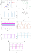
(a) Decomposition of the TA-SDR into its SET (blue trace) and RESET (red trace) contributions, here plotted together on the |x¯˙| versus x¯ plane to visualise each possible equilibrium x¯eq of equation (10), where x¯˙SET=-x¯˙RESET, for a case study, where the proposed methodology from section 5.3 set the values for the parameters V+,1, V+,2, V+,3, r+,1, r+,2, and r+,3 of a four-pulse-per-cycle pulse train voltage stimulus, with V- preliminarily chosen as -0.5V, to +0.490V, +0.649V, +0.778V, 4.594, 1.489×10⁻¹⁸, and 1.361×10-47, respectively, so as to endow the TA-SE with the 3 stable equilibria x¯eq,1=0.3, x¯eq,3=0.5, and x¯eq,7=0.7, which in turn place the maxima of the first, second, and third gaussian bells at xmax,1=0.269, xmax,2=0.469, and xmax,3=0.669. The TA-SE equilibria are found to lie at x¯eq,1=0.3, x¯eq,2=0.427, x¯eq,3=0.5, x¯eq,4=0.635, and x¯eq,5=0.7, the odd numbered of which are LAS, as requested. (b) TA-SDR of the ReRAM cell under a voltage excitation signal from the class identified by the aforegiven parameter set of cardinality 7. (c) Time waveform of a particular generalised pulse train voltage stimulus vS, extracted from the class under focus by setting τ- to 1×10⁻⁸s, which directly fixes τ+,1, τ+,2, and τ+,3 to 4.594×10⁻⁸s, 1.489×10⁻²⁶s, and 1.361×10-55s, respectively. (d) SCPCM of the ReRAM cell, subject to the specific generalised pulse train from (c), confirming the predictions drawn from the TA-SDR analysis. (e) Transients in the memory state x of the ReRAM cell, as resulting from numerical simulations of the Strachan model, with v taken identically equal to the excitation signal vS from (c), for each initial condition x0 from the set {x0,1,x0,2,x0,3,x0,4,x0,5,x0,6}={0.15,0.415,0.425,0.620,0.626,0.8}. From either of the first two, of the second two, and of the last two initial conditions the memory state of the ReRAM cell asymptotically approaches the steady-state oscillatory solutions xss,1, xss,3, and xss,5, which revolve approximately around x¯eq,1, x¯eq,3, and x¯eq,5, respectively, as illustrated in turn in plots (f), (g), and (h), visualising also their time averages x¯ss,1, x¯ss,3, and x¯ss,5, and the corresponding stable map fixed points x1, x3, and x5.
Figure 14
Figure 14
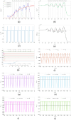
(a) Blue (Red) trace: |x¯˙SET| (|x¯˙RESET| versus x¯ locus resulting from the application of the theoretical methodology from section 5.3 to the Strachan model so as to endow the TA-SE with 4 stable equilibria x¯eq,1, x¯eq,3, x¯eq,5, and x¯eq,7 at 0.3, 0.45, 0.6, and 0.75, respectively. First the maxima xmax,1, xmax,2, xmax,3, and xmax,4 of the four gaussian bells were in turn positioned at 0.269, 0.419, 0.569, and 0.719. The amplitudes V+,1, V+,2, V+,3, and V+,4 of the four positive pulses were then chosen as 0.490V, 0.613V, 0.717V, and 0.807V, while V- was preliminarily fixed to -0.5V. Finally, the first, second, third, and fourth pulse width ratios r+,1, r+,2, r+,3, and r+,4 were respectively taken as 4.312, 6.162×10⁻¹³, 8.667×10⁻³², and 1.802×10-56. The TA-SE admits equilibria at x¯eq,1=0.3, x¯eq,2=0.372, x¯eq,3=0.45, x¯eq,4=0.532, x¯eq,5=0.6, x¯eq,6=0.684, x¯eq,7=0.75, of which those labeled with odd numbers are LAS, as desired. (b) TA-SDR of the ReRAM cell subject to any input train featuring the aforementioned 9 parameters. (c) Time course of a particular pulse train extracted from the class by fixing the RESET pulse width τ- to 1×10⁻⁸s, which automatically sets the the widths τ+,1, τ+,2, τ+,3, and τ+,4 of the four SET pulses to 4.312×10⁻⁸s, 6.162×10⁻²¹s, 8.667·10-40s, and 1.802×10-64s, respectively. (d) SCPCM of the ReRAM cell, when its voltage v is forced to follow the generalised pulse train stimulus vS from (c) at all times, validating the TA-SDR analysis. (e) Solution to the ODE (1), with state evolution function (3), under the periodic stimulus from (c), and for each initial condition x0 from the set {x0,1,x0,2,x0,3,x0,4,x0,5,x0,6,x0,7,x0,8}={0.15,0.365,0.375,0.52,0.535,0.67,0.685,0.8}. As may be evinced by monitoring the time course of the respective traces, the first, second, third, and fourth pair of initial conditions from this set respectively lie in the basins of attraction of the asymptotic memory state solutions x1,ss, x3,ss, x5,ss, and x7,ss, which in turn oscillate about the stable TA-SE equilibria x¯eq,1, x¯eq,3, x¯eq,5, and x¯eq,7, as may be inferred by inspecting plots (f), (g), (h), and (i), which also report their mean values x¯1,ss, x¯3,ss, x¯5,ss, and x¯7,ss, and the associated stable map fixed points x1, x3, x5, and x7.
Figure 15
Figure 15
Moduli of the scaled SET (blue trace) and RESET (red trace) components of the TA-SE of the ReRAM cell subject to a six-pulse-per-cycle pulse train voltage stimulus from a class identified via the 11 parameters V+,1=0.490V, V+,2=0.598V, V+,3=0.690V, V+,4=0.772V, V+,5=0.847V, r+,1=3.764, r+,2=6.651×10⁻¹¹, r+,3=3.241×10⁻²⁶, r+,4=6.156×10-46, and r+,5=5.530×10-70, and V-=-0.5V. While the last one was preliminarily chosen, the first 10 parameters were automatically determined via the analytical procedure outlined in section 5.3 so as to ensure Eq. (10) admits the 5 stable equilibria x¯eq,1=0.3, x¯eq,3=0.43, x¯eq,5=0.56, x¯eq,7=0.69, and x¯eq,9=0.82, which consequently fixed the maxima of the positive gaussian bells at xmax,1=0.269, xmax,2=0.399, xmax,3=0.529, xmax,4=0.659, and xmax,5=0.789. The TA-SE is found to feature 5 LAS equilibria at the earlier prescribed locations, and unstable ones at x¯eq,2=0.349, x¯eq,4=0.491, x¯eq,6=0.625, and x¯eq,8=0.750. (b) TA-SDR of the ReRAM cell under a periodic pulse train from the above defined class. (c) Time waveform of a particular voltage excitation signal vS, extracted from the aforementioned class by fixing the RESET pulse width τ- to 2.5×10⁻⁹s, which automatically set the widths of the five SET pulses τ+,1, τ+,2, τ+,3, τ+,4, and τ+,5 to 9.410×10⁻⁹s, 1.663×10⁻¹⁹s, 8.103×10⁻³⁵s, 1.539×10-54s, and 1.383×10-78s, respectively. (d) SCPCM of the ReRAM cell subject to the particular generalised pulse train voltage stimulus from (c), confirming the predictive capability of the TA-SDR analysis tool. (e) Time evolution of the memory state x of the ReRAM cell, as observed in numerical simulations of the Strachan model, where v was constrained to follow the voltage stimulus vS from (c) at all times, and for each initial condition x0 from the set {x0,1,x0,2,x0,3,x0,4,x0,5,x0,6,x0,7,x0,8,x0,9,x0,10}={0.15,0.34,0.35,0.485,0.49,0.62,0.625,0.745,0.75,0.9}. When initiated from either initial condition in the first, second, third, fourth, and fifth pair, the memristor state x converges progressively toward the steady-state waveforms xss,1, xss,3, xss,5, xss,7, and xss,9, respectively, as illustrated in plots (f), (g), (h), (i), and (l), which further visualise in turn the mean values x¯1,ss, x¯3,ss, x¯5,ss, x¯7,ss, and x¯9,ss of the asymptotic oscillations, together with the corresponding stable map fixed points x1, x3, x5, x7, and x9.
Figure 16
Figure 16
Illustration revealing the possible exploitation of the local history erase effects to compensate for unwanted yet unavoidable drifts in the synaptic conductances of crosspoint nanodevices under power off conditions. (a) Initial configuration of the synaptic weight matrix in a nonvolatile memory crossbar with 15 rows and 13 columns. Each of the 195 ReRAM cells, modelled via the Strachan DAE set, is preliminarily programmed in one of four states, specifically {0.3,0.45,0.6,0.75}, coinciding with the TA-SE equilibria in the case study from Fig. 14. (b) Synaptic weight matrix sampled at an arbitrary time instant, during an idle phase, following the programming step, which reveals the detrimental effect of additive noise from a uniform distribution across the range [-0.06,+0.06]. (c) Retrieval of the original synaptic weight matrix after transients decay to zero during the application of the five-pulse-per-cycle pulse train voltage stimulus vS from Fig. 14d across each of the 195 crosspoint nanodevices. (d) Time course of the states of the crosspoint nanodevices from the respective initial conditions, corresponding to the synaptic weight matrix from (b), toward asymptotic oscillations, revolving around their target values. The memory configuration in (c) is extracted by sampling simultaneously all the states of the ReRAM cells at the last time instant, corresponding to the end of an input cycle, which is shown along the horizontal axis in (d). The colour coding map, depicted in (d), applies to all the plots in this figure.

References

    1. Ielmini, D. & Waser, R. Resistive Switching: From Fundamentals of Nanoionic Redox Processes to Memristive Device Applications 1st edn. (Wiley, 2016).
    1. Corinto, F., Forti, M. & Chua, L. Nonlinear Circuits and Systems with Memristors: Nonlinear Dynamics and Analogue Computing via the Flux-Charge Analysis Method 1st edn. (Springer, 2021).
    1. Ascoli, A., Tetzlaff, R., Chua, L., Strachan, J. & Williams, R. History erase effect in a non-volatile memristor. IEEE Trans. Circuits Syst.I(63), 389–400 (2016).10.1109/TCSI.2016.2525043 - DOI
    1. Strachan, J. et al. State dynamics and modeling of tantalum oxide memristors. IEEE Trans. Electron. Devices60, 2194–2202 (2013).10.1109/TED.2013.2264476 - DOI
    1. Ascoli, A., Tetzlaff, R., Chua, L., Strachan, J. & Williams, R. Memory loss in a tantalum oxide memristor. In Advances in Science and Technology, Proceedings of International Conference on Smart Materials, Structures and Systems (Perugia, Italy, 5–9 June 2016), vol. 99, 94–101 (Trans Tech Publications, 2017).