. 2024 Jul;16(7):1133-1140.
doi: 10.1038/s41557-024-01477-1. Epub 2024 Mar 8.

Porphyrin-fused graphene nanoribbons

Affiliations

Porphyrin-fused graphene nanoribbons

Qiang Chen et al. Nat Chem. 2024 Jul.

Abstract

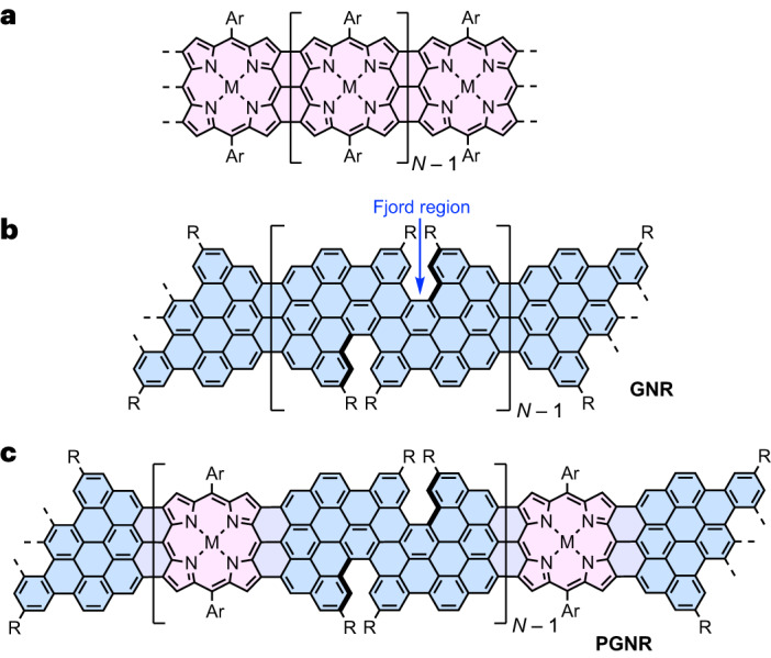
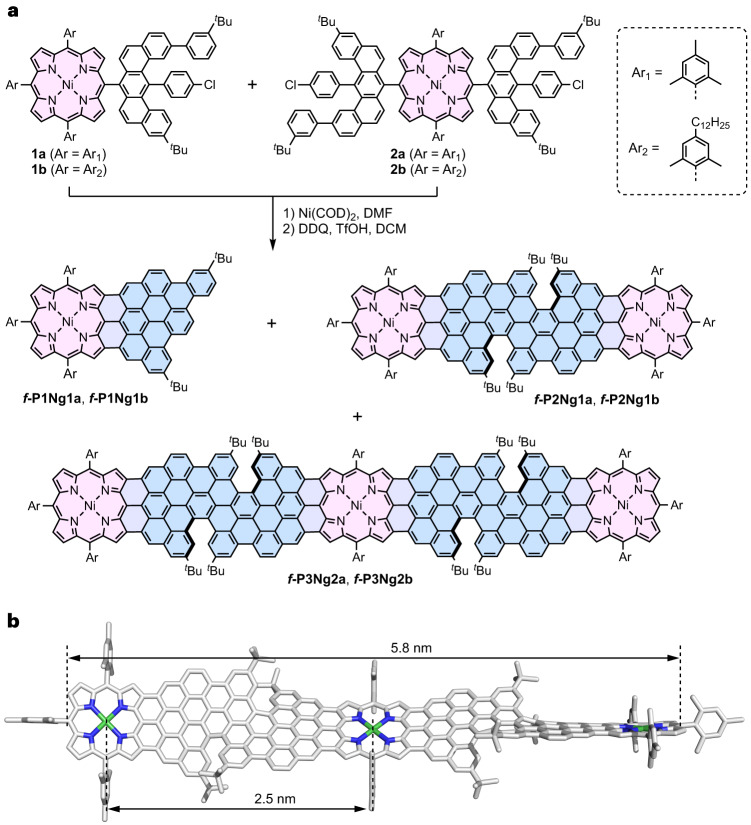
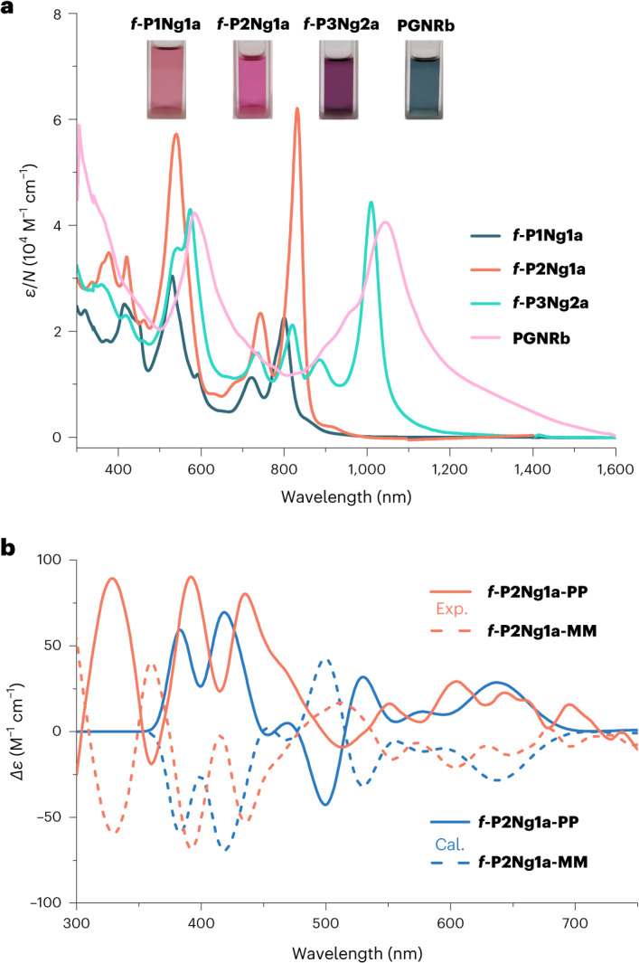
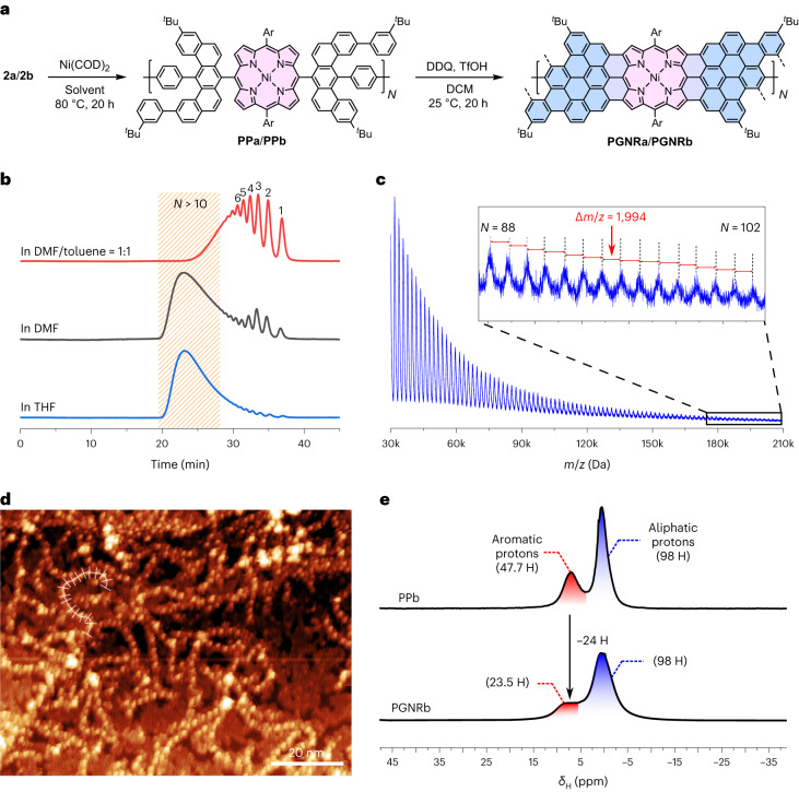
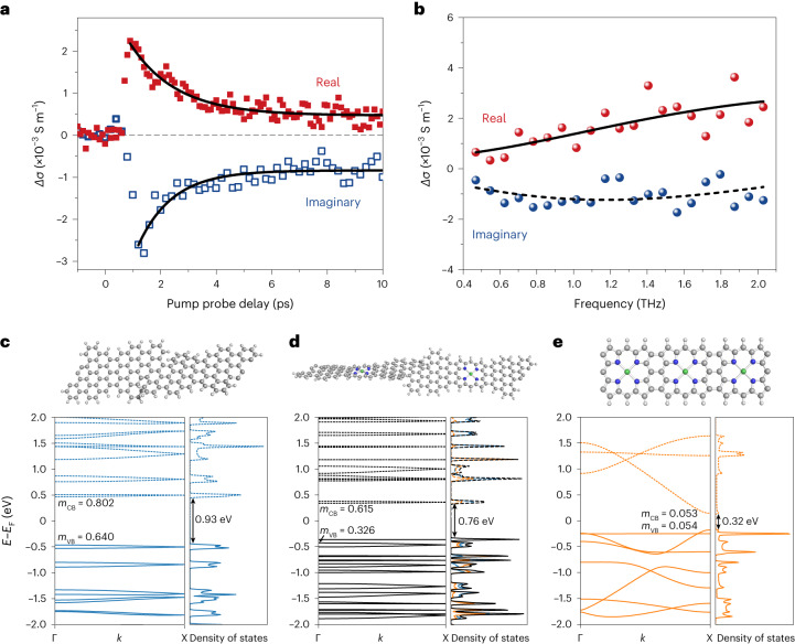
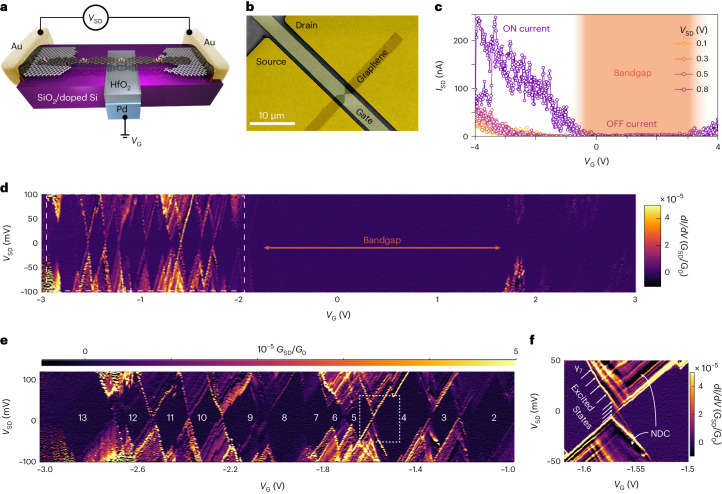
Graphene nanoribbons (GNRs), nanometre-wide strips of graphene, are promising materials for fabricating electronic devices. Many GNRs have been reported, yet no scalable strategies are known for synthesizing GNRs with metal atoms and heteroaromatic units at precisely defined positions in the conjugated backbone, which would be valuable for tuning their optical, electronic and magnetic properties. Here we report the solution-phase synthesis of a porphyrin-fused graphene nanoribbon (PGNR). This PGNR has metalloporphyrins fused into a twisted fjord-edged GNR backbone; it consists of long chains (>100 nm), with a narrow optical bandgap (~1.0 eV) and high local charge mobility (>400 cm2 V-1 s-1 by terahertz spectroscopy). We use this PGNR to fabricate ambipolar field-effect transistors with appealing switching behaviour, and single-electron transistors displaying multiple Coulomb diamonds. These results open an avenue to π-extended nanostructures with engineerable electrical and magnetic properties by transposing the coordination chemistry of porphyrins into graphene nanoribbons.


Conflict of interest statement

The authors declare no competing interests.

Figures

Fig. 1
Fig. 1. The design concept.
a, Edge-fused porphyrin ribbon. b, Graphene nanoribbon with fjord-type edges. c, Porphyrin-fused fjord-edged graphene nanoribbon. The porphyrin and graphene nanoribbon moieties are highlighted in pink and blue, respectively. R = tBu- and Ar = bulky substituted phenyl.
Fig. 2
Fig. 2. Synthesis of porphyrin-fused nanographene oligomers as model compounds.
a, Synthetic route to f-P1Ng1, f-P2Ng1 and f-P3Ng2. COD, 1,5-cyclooctadiene; DMF, N,N-dimethylformamide; DDQ, 2,3-dichloro-5,6-dicyano-1,4-benzoquinone; TfOH, trifluoromethanesulfonic acid; DCM, dichloromethane. b, DFT-optimized geometry of f-P3Ng2a (M,M,M,M configuration), showing the twisted edge structure, the molecular size and the distance between two porphyrin centres. Source data
Fig. 3
Fig. 3. Room-temperature optical properties.
a, Ultraviolet–visible–near infrared absorption spectra of f-P1Ng1a, f-P2Ng1a and f-P3Ng2a (in chloroform, c = 10–5 M) and PGNRb (in 1,2,4-trichlorobenzene, c = 0.025 mg ml–1). The molar absorption coefficient is normalized by the number of porphyrin units in each molecule, N. Photographs of the solutions are shown in the inset. b, Circular dichroism spectra (orange) of the two enantiomers of f-P2Ng1a measured in chloroform (c = 10–5 M), and the TD-DFT-calculated spectra using the LC-ωHPBE (ω = 0.1) functional (blue). Source data
Fig. 4
Fig. 4. Synthesis and structural characterization of PGNRs.
a, Synthesis of PGNRs, with the porphyrin and graphene nanoribbon moieties highlighted in pink and blue, respectively. b, Analytical GPC traces of Yamamoto polymerization products of dichloroporphyrin 2b from reaction in DMF/toluene (1:1, v/v), DMF and THF (eluent: THF/1% pyridine, flow rate = 1 ml min–1, detection at 430 nm). Peaks are labelled with N, the number of repeat units. c, MALDI-TOF mass spectrum of PPb measured with trans-2-[3-(4-tert-butylphenyl)-2-methyl-2-propenylidene]malononitrile (DCTB) as the matrix, conducted in the linear mode. Peaks from the polymer extend up to a molecular weight of 210 kDa (102 repeat units) and the average m/z difference between neighbouring peaks corresponds to one repeat unit. d, STM topograph of PPa transferred from toluene solution to a Au(111) surface via electro-spray deposition, and subsequently annealed to 250 °C (Tsample = 4.7 K, Vsample-bias = 2 V, Iset-point = 50 pA). e, CP-MAS solid-state 1H-NMR spectra of PPb in comparison with PGNRb, and the integration of protons in the aromatic and aliphatic regions. Source data
Fig. 5
Fig. 5. Ultrafast photoconductivity by terahertz spectroscopy and band structure.
a, Time-resolved complex photoconductivity dynamics of PGNRb measured in 1,2,4-trichlorobenzene (0.33 mg ml–1) at room temperature. The solid lines represent fitted photoconductivity dynamics by a single-exponential decay (+long-lived offset) with the same decay time of 1.5 ± 0.2 ps for both the real and imaginary parts. b, Frequency-resolved terahertz photoconductivity of PGNRb measured at tp = 2 ps. The data are fitted by the Drude–Smith model described in the main text. c–e, Energy bands as a function of the wavevector k and density of states of GNR (c), PGNR (d) and porphyrin ribbon (e). The energy band gap (Eg), valence and conduction bands, and effective mass (mCB and mVB) are shown; energies are reported relative to the intrinsic Fermi level (EF). The colour scale for PGNR represents the proportion of electron density on GNR (blue) or porphyrin (orange); occupied (unoccupied) levels are shown as solid (dotted) lines. Source data
Fig. 6
Fig. 6. Single-molecule charge transport.
a, Scheme of the electronic devices, where a single strand of PGNRb bridges two graphene electrodes (separated by a nanogap) connected to gold pads. A palladium gate is deposited on the SiO2/Si surface and covered with a 10-nm-thick HfO2 dielectric. b, False-colour scanning electron image of a typical device, showing the pads, graphene electrodes and gate. c, Characteristic curve for a field-effect transistor obtained with a single PGNRb at room temperature and a VG sweep rate of 44 mV s–1 for various source-drain voltages. The electronic bandgap region and the ON and OFF states are highlighted. d, Single-electron transistor map of the differential conductance GSD (colour scale bar, in units of the quantum of conductance G0) observed at 25 mK. e, Enlarged view of the Coulomb blockade regions, with the number of holes highlighted. f, Enlarged view of the region enclosed within the dashed white box in e, showing vibrational sublevels and negative differential conductance regions (labelled NDC). Source data

References

    1. Nakada K, Fujita M, Dresselhaus G, Dresselhaus MS. Edge state in graphene ribbons: nanometer size effect and edge shape dependence. Phys. Rev. B. 1996;54:17954–17961. - PubMed
    1. Son YW, Cohen ML, Louie SG. Energy gaps in graphene nanoribbons. Phys. Rev. Lett. 2006;97:216803. - PubMed
    1. Houtsma RSK, de la Rie J, Stohr M. Atomically precise graphene nanoribbons: interplay of structural and electronic properties. Chem. Soc. Rev. 2021;50:6541–6568. - PMC - PubMed
    1. Wang H, et al. Graphene nanoribbons for quantum electronics. Nat. Rev. Phys. 2021;3:791–802.
    1. Jiao L, Wang X, Diankov G, Wang H, Dai H. Facile synthesis of high-quality graphene nanoribbons. Nat. Nanotechnol. 2010;5:321–325. - PubMed

LinkOut - more resources