Review
. 2024 Feb 27;24(5):1529.
doi: 10.3390/s24051529.

On-Chip Photonic Detection Techniques for Non-Invasive In Situ Characterizations at the Microfluidic Scale

Affiliations
Review

On-Chip Photonic Detection Techniques for Non-Invasive In Situ Characterizations at the Microfluidic Scale

Tamar Kurdadze et al. Sensors (Basel). .

Abstract

Microfluidics has emerged as a robust technology for diverse applications, ranging from bio-medical diagnostics to chemical analysis. Among the different characterization techniques that can be used to analyze samples at the microfluidic scale, the coupling of photonic detection techniques and on-chip configurations is particularly advantageous due to its non-invasive nature, which permits sensitive, real-time, high throughput, and rapid analyses, taking advantage of the microfluidic special environments and reduced sample volumes. Putting a special emphasis on integrated detection schemes, this review article explores the most relevant advances in the on-chip implementation of UV-vis, near-infrared, terahertz, and X-ray-based techniques for different characterizations, ranging from punctual spectroscopic or scattering-based measurements to different types of mapping/imaging. The principles of the techniques and their interest are discussed through their application to different systems.

Keywords: analytical chemistry; lab-on-a-chip; microfluidics; photonic detection; sensors; spectrometry.


Conflict of interest statement

The authors declare no conflicts of interest.

Figures
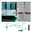
Figure 5
Figure 5
(a) Three-dimensional microlens-incorporating microfluidic chip (3D-MIMC) with large optical path length and incorporated optical fiber. Reproduced from [124], from the journal Lab on a Chip published by the Royal Society of Chemistry 2020. (b) Enlarging the optical path length of the droplet by using droplet stretching for high-sensitivity measurements. Figure adapted from [128], from the journal Analytical Chemistry published by the American Chemical Society 2021. Copyright 2017 American Chemical Society. (c) UV–vis spectra activated droplet sorter (UVADS) for high-throughput label-free chemical identification and enzyme screening. Adapted with permission from [126]. Copyright 2017 American Chemical Society.
Figure 1
Figure 1
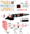
(a) Scheme of the custom-made microscope used for imaging of Drosophila embryos. Reproduced from [67], from Journal of BIOphotonics published by Wiley 2020. (b) Schematic design of SLS-IFC platform: a PM fiber is coupled to an integrated optical circuit designed to symmetrically split the beam and introduce an on-demand phase shift between the two outputs. The collected signal, transmitted through PM fibers, reaches an optofluidic chip, where microlenses generate two overlapping light sheets within a microfluidic channel, forming patterned illumination light. Reproduced from [68], from the journal Lab on a Chip published by the Royal Society of Chemistry 2024.
Figure 2
Figure 2
Schematic of ATR-FTIR imaging system integrated with a planar microfluidic chip. Reproduced from [104] with permission from the Royal Society of Chemistry. Copyright 2009; permission conveyed through Copyright Clearance Center, Inc.
Figure 3
Figure 3
(a) Schematic representation of the microfluidic device integrated with automated droplet sampling and THz measurements. (b) Refractive index spectra of liver cancer cells after treatment by resveratrol drug for 0, 12, and 24 h. Figure adapted from [115], from the journal Frontiers in Bioengineering and Biotechnology, section Nanobiotechnology published by Frontiers 2023.
Figure 4
Figure 4
Schematic representation of the OCER platform: 1. inlet ports; 2. additional inlet port; 3. passive zigzag micromixer; 4. serpentine channel for droplet storage (2000 droplets of 2 nL) featuring a cross-sectional view of the solution-storage layout for enzyme crystallization and further cross-linking of the crystals; 5. structures before and after serpentine channel to prevent the dragging of non-fixed crystals/aggregates by injected solutions; 6. Outlet for the crystallization and cross-linking solution to avoid contamination of sensing region; 7. multiple path configuration for the photonic detection system, enabling exploration of a wide concentration range; 8. in red: 2D microlenses with air mirrors along the interrogation channel to prevent cross-talking, self-alignment elements for fiber optics alignment and clamping. Fiber optics are connected to an external light source and spectrometer for on-chip real-time analyses; 9. outlet port for the product solutions. Reprinted with permission from [123]. Copyright 2016 American Chemical Society.
Figure 6
Figure 6
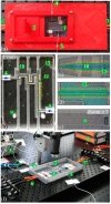
Experimental setup for the photonic lab-on-a-chip with three optical path lengths used for light extinction spectrometry measurements. (a) global view of the device in a 3D-Printed hausing; (b) detailed view of the chip. (1) Glass chip in its (2) housing (hatch open); (3) computer-controlled syringe pumps (×2) feeding the LoC via its (4) inlet and (5) outlet; (6,7) optical fiber connections; (8) CCD spectrometers. (ce) Expanded views of (9) the self-alignment channels (×6) for optical fibers; (10) two-dimensional collimating microlens assemblies; (11) optical channels with path lengths L = 1.0, 3.5, and 10 mm, width 650 µm, and depth 250 µm; (12) channels’ end with parallel optical-grade windows; (13) air channels to avoid probing channels cross-talking during simultaneous acquisition. (f) Setup with (2) LoC housing cover removed. Reproduced from [136], from the journal Optics Express published by Optica Publishing group 2022.
Figure 7
Figure 7
The schematic representation of nanoparticle detection by thermal lens microscope (TLM). No thermal lens effect occurs when there are no nanoparticles present (left). The probe beam is deflected due to the thermal lens effect, causing deviation in probe beam intensity after the pinhole (right). Reprinted from [138]. Copyright (2016), with permission from Elsevier.
Figure 8
Figure 8
(a) Schematic representation of on-chip fluorescence detection in droplet microfluidics with an integrated microlens and a metallic mirror. (b) Comparison of fluorescence intensity obtained by the conventional device and the chip integrated with micro-optics. Figure adapted from [144], from the journal Lab on a Chip published by the Royal Society of Chemistry 2013.
Figure 9
Figure 9
Microchip design and fabrication schematics proposed by Gavira and coworkers for in situ XRD. (a,b) Operation scheme of a PDMS mold over a Kapton/Mylar film. Liquid OSTEMER formulation fills the gaps between the mold and the Kapton/Mylar film by diffusing by capillary action. (c) After UV exposure for OSTEMER cross-linking, the PDMS mold is removed, and the resulting structure is glued to a second Kapton/Mylar film. (d). Final view of the X-ray transparent chips, scale bar representing 1 cm. Figure reproduced from [170] with permission from the International Union of Crystallography.
Figure 10
Figure 10
(a) Schematics of the droplet-based microfluidic platform proposed by Rodriguez-Ruiz et al., to study protein interactions in solution by combining on-line UV–vis concentration measurements and SAXS [127]. Protein solution droplets at different concentrations are generated and monitored by continuous sensing in the microfluidic platform. Subsequently, they are sent to the SAXS sample holder, where measurements are synchronized with the droplets in movement by actuating in the beam shutter. (b) Picture and details of the microfluidic platform showing (1) interrogation areas for photonic detection (detailed in figure inset, where A, B and C inlets are protein, buffer, and precipitant solutions, respectively), (2) serpentine channel for droplet storage, and (3) inlets for temperature probes.
Figure 11
Figure 11
(a) Scanning electron microscopy (SEM) image of the lens system incorporating the notch filter. (b) Ray-trace simulation of the notch filter in the lens system showing the light gap created in the image plane. Figure adapted from [181], from the journal Biomedical Optics Express published by Optica Publishing Group 2013.
Figure 12
Figure 12
Principle of holographic characterization: (1) experimental setup; (2) normalized hologram of a polystyrene microbead in water and corresponding fit of the experimental hologram to the prediction of the Lorenz–Mie scattering theory; (3) radial profile of the experimental hologram (black) of polystyrene bead dispersed in water overlaid with the fit profile (orange), showing excellent agreement. The blue-shaded region corresponds to the instrumental uncertainty. (4) Distribution of three distinct populations of spheres. Figure adapted from [184], from the journal Water Research published by Elsevier 2017.
Figure 13
Figure 13
(a) The optical interrogation region of the multiparametric optofluidic chip for absorption, fluorescence, and light scattering measurements. Reproduced from [195], from the journal Biomicrofluidics published by AIP Publications 2020. (b) Schematic diagram of a MALS microscope setup for on-chip measurements. Reprinted from [196], copyright 2017, with permission from Elsevier. (c) The µSFC setup: the laser beam is directed at a 40° angle onto the microfluidic channel, positioned 400 µm away from the microscope objective’s focal plane. The objective collects light scattered by particles and focuses it through a lens onto a slit in front of a detector. The virtual image of the slit selects various scattering angles at different positions along particle trajectories. These angles are presented at distinct positions in the back focal plane of the objective, reaching the detector at varying times. To enhance the measurement’s signal-to-noise ratio, a filter with a linearly variable optical density in the back focal plane of the objective reduces the dynamic range. Reproduced from [197], from the journal Lab on a Chip published by the Royal Society of Chemistry 2023.

Similar articles

Cited by

References

    1. Manz A., Graber N., Widmer H.M. Miniaturized Total Chemical Analysis Systems: A Novel Concept for Chemical Sensing. Sens. Actuators B Chem. 1990;1:244–248. doi: 10.1016/0925-4005(90)80209-I. - DOI
    1. Gravesen P., Branebjerg J., Jensen O.S. Microfluidics—A Review. J. Micromech. Microeng. 1993;3:168. doi: 10.1088/0960-1317/3/4/002. - DOI
    1. Zhou S., Chen B., Fu E.S., Yan H. Computer Vision Meets Microfluidics: A Label-Free Method for High-Throughput Cell Analysis. Microsyst. Nanoeng. 2023;9:116. doi: 10.1038/s41378-023-00562-8. - DOI - PMC - PubMed
    1. Lin P.H., Nien H.H., Li B.R. Wearable Microfluidics for Continuous Assay. Annu. Rev. Anal. Chem. 2023;16:181–203. doi: 10.1146/annurev-anchem-091322-082930. - DOI - PubMed
    1. Ma Y., Liu C., Cao S., Chen T., Chen G. Microfluidics for Diagnosis and Treatment of Cardiovascular Disease. J. Mater. Chem. B. 2022;11:546–559. doi: 10.1039/D2TB02287G. - DOI - PubMed

LinkOut - more resources