. 2024 Mar 27;24(12):3575-3580.
doi: 10.1021/acs.nanolett.3c04002. Epub 2024 Mar 13.

Plasmonic Diamond Membranes for Ultrafast Silicon Vacancy Emission

Affiliations

Plasmonic Diamond Membranes for Ultrafast Silicon Vacancy Emission

Andrew M Boyce et al. Nano Lett. .

Abstract

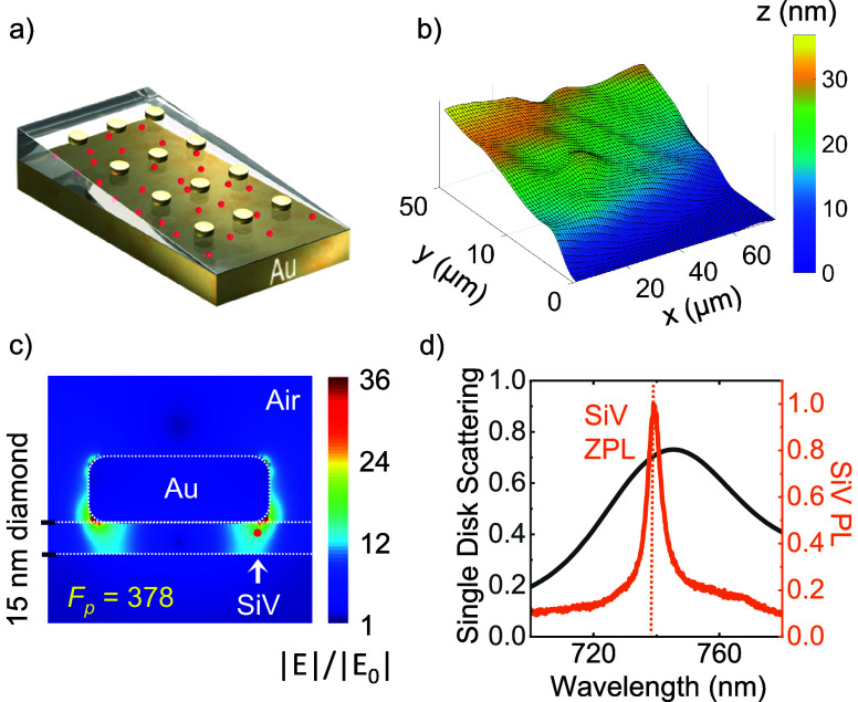
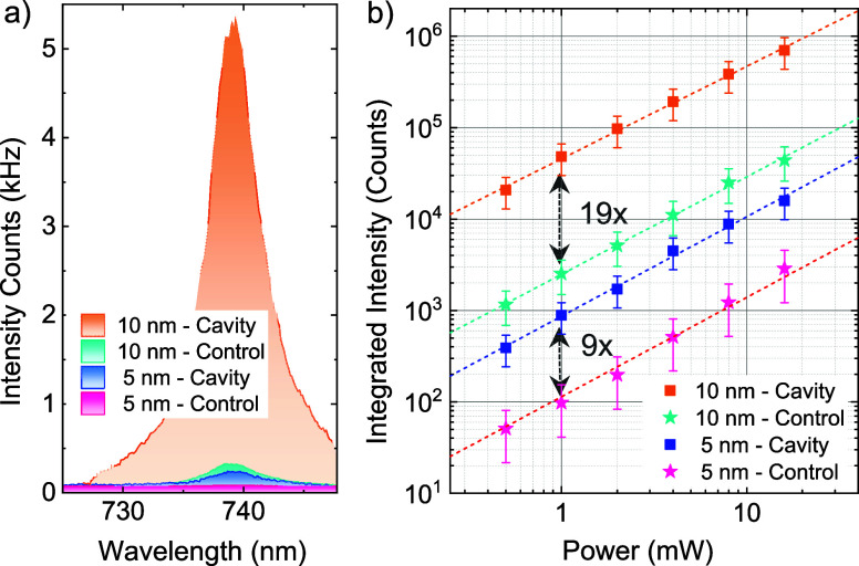
Silicon vacancy centers (SiVs) in diamond have emerged as a promising platform for quantum sciences due to their excellent photostability, minimal spectral diffusion, and substantial zero-phonon line emission. However, enhancing their slow nanosecond excited-state lifetime by coupling to optical cavities remains an outstanding challenge, as current demonstrations are limited to ∼10-fold. Here, we couple negatively charged SiVs to sub-diffraction-limited plasmonic cavities and achieve an instrument-limited ≤8 ps lifetime, corresponding to a 135-fold spontaneous emission rate enhancement and a 19-fold photoluminescence enhancement. Nanoparticles are printed on ultrathin diamond membranes on gold films which create arrays of plasmonic nanogap cavities with ultrasmall volumes. SiVs implanted at 5 and 10 nm depths are examined to elucidate surface effects on their lifetime and brightness. The interplay between cavity, implantation depth, and ultrathin diamond membranes provides insights into generating ultrafast, bright SiV emission for next-generation diamond devices.

Keywords: Purcell enhancement; diamond; nanocavity; plasmonics; silicon vacancy.


Conflict of interest statement

The authors declare no competing financial interest.

Figures

Figure 1
Figure 1
Sample fabrication overview. (a) Fabrication process for creating nanogap cavities with embedded SiVs. (b) Optical microscope image of the etched diamond slab after transfer onto a gold film. (c) SEM image of gold nanodisks after EBL fabrication on silicon.
Figure 2
Figure 2
Approach for integration of SiVs in diamond into plasmonic nanogap cavities. (a) Schematic of sample structure consisting of Au nanodisks (30 nm height and 95 nm diameter) separated from an Au ground plane by an etched diamond slab. (b) Height profile of the thinnest part of the diamond slab measured using an imaging ellipsometer, with minimum thickness ∼10–20 nm (c) Electric field profile of the structure simulated via finite-difference, time-domain methods using a 738 nm normal incident plane wave (see SI). (d) Single disk scattering spectrum (black) overlaid with a PL spectrum of embedded SiVs (orange), showing good spectral overlap.
Figure 3
Figure 3
Time-resolved fluorescence lifetime from SiVs coupled to single nanocavities and a metasurface. (a) SiV lifetimes show biexponential decays from a single cavity (10 nm depth—orange, and 5 nm depth—blue) and 10 nm depth coupled to a metasurface (magenta). Lifetime for SiVs in diamond on silicon (control sample) exhibits similar single exponential decay (turquoise) for both depths, system IRF is displayed in gray. Inset: log plot highlighting the slow lifetime component of the 5 nm single cavity and 10 nm metasurface samples. (b) Histogram of τfast distribution for all three samples. Most spots from both single cavity samples exhibit τfast ≤ 8 ps, which is limited by the 4 ps bin size of the TCSPC system and is extracted via iterative reconvolution of a biexponential fit with the system IRF.
Figure 4
Figure 4
SiV PL power dependence of 10 and 5 nm implantation depth. (a) Example SiV intensity/s when SiVs are excited at 1 mW. (b) Integrated photon counts/s with 514 nm CW laser excitation from 0.5 mW to 16 mW on both sets of samples.

References

    1. Sipahigil A.; Jahnke K. D.; Rogers L. J.; Teraji T.; Isoya J.; Zibrov A. S.; Jelezko F.; Lukin M. D. Indistinguishable Photons from Separated Silicon-Vacancy Centers in Diamond. Phys. Rev. Lett. 2014, 113 (11), 113602.10.1103/PhysRevLett.113.113602. - DOI - PubMed
    1. Somaschi N.; Giesz V.; De Santis L.; Loredo J. C.; Almeida M. P.; Hornecker G.; Portalupi S. L.; Grange T.; Antón C.; Demory J.; Gómez C.; Sagnes I.; Lanzillotti-Kimura N. D.; Lemaítre A.; Auffeves A.; White A. G.; Lanco L.; Senellart P. Near-Optimal Single-Photon Sources in the Solid State. Nat. Photonics 2016, 10 (5), 340–345. 10.1038/nphoton.2016.23. - DOI
    1. Huber D.; Reindl M.; Huo Y.; Huang H.; Wildmann J. S.; Schmidt O. G.; Rastelli A.; Trotta R. Highly Indistinguishable and Strongly Entangled Photons from Symmetric GaAs Quantum Dots. Nat. Commun. 2017, 8 (1), 15506.10.1038/ncomms15506. - DOI - PMC - PubMed
    1. Sun S.; Kim H.; Luo Z.; Solomon G. S.; Waks E. A Single-Photon Switch and Transistor Enabled by a Solid-State Quantum Memory. J. Phys. B At. Mol. Opt. Phys. 2018, 361 (6397), 57–60. 10.1126/science.aat3581. - DOI - PubMed
    1. Sukachev D. D.; Sipahigil A.; Nguyen C. T.; Bhaskar M. K.; Evans R. E.; Jelezko F.; Lukin M. D.. Silicon-Vacancy Spin Qubit in Diamond: A Quantum Memory Exceeding 10 Ms with Single-Shot State Readout. Phys. Rev. Lett. 2017, 119 ( (22), ), 223602.10.1103/PhysRevLett.119.223602. - DOI - PubMed