. 2024 Feb 6;6(6):1704-1719.
doi: 10.1039/d3na01105d. eCollection 2024 Mar 12.

Influence of arylalkyl amines on the formation of hybrid CsPbBr3 nanocrystals via a modified LARP method

Affiliations

Influence of arylalkyl amines on the formation of hybrid CsPbBr3 nanocrystals via a modified LARP method

Ernest Ruby et al. Nanoscale Adv. .

Abstract

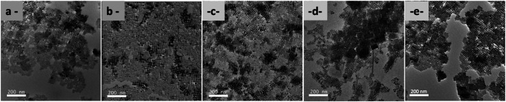
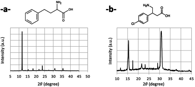
Perovskite nanocrystals have attracted much attention in the last ten years due to their different applications, especially in the photovoltaic domain and LED performance. In this large family of perovskite nanocrystals, CsPbBr3 nanocrystals are attractive nanomaterials because they are good candidates for obtaining green emissions and exploring new synthesis routes. In this context, controlling the nanometric scale's morphology, particularly the size and monodispersity, is fundamental for exploring their photophysical properties and final applications. Currently, the nanometric size of nanocrystals is ensured by the presence of oleic acid and oleylamine molecules, in using Hot Injection (HI) or ligand-assisted reprecipitation (LARP) methods. If oleic acid plays a fundamental role, oleylamine can be easily substituted by other amino molecules, opening the way for the functionalization of CsPbBr3 nanocrystals and the obtention of new hybrid perovskite nanocrystal families. In this article, we describe the synthesis, by soft chemistry, of a new family of hybrid organic-inorganic CsPbBr3 nanocrystals, functionalized by aryl-alkylamine (AAA) molecules, through the modified LARP method. We highlight the mechanism for cutting submicron crystals into nanocrystals, using aryl-alkylamine molecules like scissors. The impact of these amino molecules on the final nanocrystals leads to different nanocrystal morphologies (nanocubes, nanosheets, or nanorods) and structures (monoclinic, rhombohedral, or tetragonal). In addition, this modified LARP method highlights, under certain experimental conditions, an unexpected formation of PbO ribbons.


Conflict of interest statement

6There are no conflicts to declare.

Figures

Scheme 1
Scheme 1. Summary of the AAA molecules studied in this work.
Scheme 2
Scheme 2. Schematic representation of the synthesis of these high-calibrated nanocrystals.
Fig. 1
Fig. 1. HAADF-STEM analysis of CF3PEA-NCs (scale bar: 30 nm): (a) scheme of the molecule; (b) in HAADF and by EDS to visualize (c) Pb element; (d) F element; (e) Br element; and (f) Cs element.
Fig. 2
Fig. 2. TEM (200 kV) images (scale bar: 200 nm) of (a) PMA-NCs; (b) tBuPMA-NCs; (c) MeOPMA-NCs; (d) NaphPMA-NCs; and (e) ThioMA-NCs.
Scheme 3
Scheme 3. Schematic representation of the starting 3D-superlattice of Naph–PMA nanocrystals and the corresponding TEM pictures.
Fig. 3
Fig. 3. TEM images (200 kV) of CF3–PMA nanocrystals, (a) scale bar 100 nm and (b) scale bar 200 nm.
Fig. 4
Fig. 4. XRD patterns of (a) tBuPMA-NCs, (b) MeOPMA-NCs, and (c) PhPMA-NCs.
Fig. 5
Fig. 5. TEM (200 kV) pictures of Thio–EA nanocrystals with scale bar (a) 500 nm and (b) 200 nm.
Fig. 6
Fig. 6. TEM analysis of DPEA-NCs (a) by TEM (200 kV, scale bar 200 nm) of long rods; (b) by TEM (200 kV, scale bar 200 nm) of small rods, and (c) by HAADF-STEM of these small rods (scale bar 20 nm).
Fig. 7
Fig. 7. (a) TEM (200 kV) pictures of AcAm1 (scale bar 200 nm) and (b) HRSTEM in HAADF of AcAm2 nanocrystals (scale bar 100 nm).
Fig. 8
Fig. 8. XRD patterns of (a) AmAc1-NCs and (b) AmAc2 NCs.
Fig. 9
Fig. 9. HAADF-STEM analysis of DPPA to highlight (a) Pb°-NP and PbO nanoribbon structures (scale bar 10 nm) and (b) assembly of PbO nanoribbon structures (scale bar 5 nm).
Fig. 10
Fig. 10. Sample SB solutions of PPA-NCs: (a) view of the solutions and the drops of PPA-2-NCs (ratio of PPA/Pb2+ = 2) and PPA-0.5-NCs (ratio of PPA/Pb2+ = 0.5), (b) lighted with a UV lamp, (c) showing the drying of a drop-in glass slide, (d) lighted with a UV lamp, (e) both solutions obtained by dissolution in toluene of both dried drops onto the glass slide and (f) lighted with a UV lamp.
Fig. 11
Fig. 11. XRD of a dried drop of (a) PPA-2 and (b) PPA-0.5 and corresponding pictures of (c) HRSTEM (scale bar 100 nm) of a dried drop of PPA-2 samples dissolved in toluene, with narrow nanowires, and (d) TEM (200 kV, scale bar 200 nm) of PPA-0.5 showing PPA-nanocrystals.
Fig. 12
Fig. 12. TEM pictures of samples obtained (a) with PEA molecules with a ratio of PEA/Pb2+ = 4 showing nanowires (scale bar 200 nm) and (b) with DPPA/Pb2+ = 2, showing undefined nanocrystals without Cs+ cations (scale bar = 5 nm) with Pb° nanoparticles.
Fig. 13
Fig. 13. HAADF-STEM analysis of PEA (ratio of PEA/Pb2+ = 4) (a) in HAADF and by EDS to visualize (b) Pb element; (c) Br element; and (d) Cs element.
Fig. 14
Fig. 14. Optical spectroscopy of PPA-nanocrystals in two different ratios: PPA-2 (ratio of PPA/Pb2+ = 2) and PPA-0.5 (ratio of PPA/Pb2+ ≈0.5); (a) absorption spectra of solutions from, in a dotted black line, 2 eq. of PPA before drying, in a red line, after drying of the drop, in a blue line, 0.5 eq. of PPA before drying, and in a green line, after drying of the drop; and (b) emission spectra (excitation at 403.5 nm) of solutions from, in a dotted black line, 2eq. of PPA before drying, in a red line, after drying of the drop, in a blue line, 0.5 eq. of PPA before drying, and in a green line, after drying of the drop.
Scheme 4
Scheme 4. Scheme of the mechanism occurring during the MLARP process, with the corresponding TEM pictures, (a) PVK TOA used first (scale bar 200 nm), (b) first action of AAA with some crystallographic lines without the Cs+ cation showing the cutting process (scale bar 10 nm), (c) detachment of new calibrated nanocrystals (scale bar 10 nm), and schematic representation of different structures of nanocrystals detected after this process with ((d)-i) representation of calibrated nanocrystals (scale bar 10 nm), ((d)-ii) similar nanocrystals with the presence of Pb° nanoparticles (scale bar 10 nm), and ((d)-iii) similar nanocrystals with the presence of PbO ribbons on the nanocrystals (scale bar 5 nm); (e) when AAA is in excess some undefined nanocrystal without Cs+ is formed (scale bar 10 nm) and (f) formation of ultimate nanowires due to AAA in excess (scale bar 200 nm).
Fig. 15
Fig. 15. HAADF-STEM of PEA nanocrystals (ratio of PEA/Pb2+ = 1) dropped on the copper grid after less than one minute of the addition of pre-SB solution, showing the different cutting areas, (a) scale bar 50 nm, (b) scale bar 10 nm and (c) scale bar 5 nm.

References

    1. Huang Q. J. Zhu Y. Adv. Mater. Technol. 2019;4:1800546. doi: 10.1002/admt.201800546. - DOI
    1. Zhang Q. Shang Q. Su R. Thu Ha Do T. Xiong Q. Nano Lett. 2021;21:1903–1914. doi: 10.1021/acs.nanolett.0c03593. - DOI - PubMed
    1. Wang Y. Song L. Chen Y. Huang W. ACS Photonics. 2020;7:10–28. doi: 10.1021/acsphotonics.9b01233. - DOI
    1. Shen W. Chen J. Wu J. Li X. Zeng H. ACS Photonics. 2021;8:113–124. doi: 10.1021/acsphotonics.0c01501. - DOI
    1. Mohammed E. Al-Qaisi S. Alrowaili Z. A. Alzaid M. Maskar E. Es-Smairi A. Vu T. V. Rai D. P. Sci. Rep. 2021;11:20622. doi: 10.1038/s41598-021-99551-y. - DOI - PMC - PubMed