. 2024 Mar 14;15(1):2334.
doi: 10.1038/s41467-024-46372-y.

Ultra-fast switching memristors based on two-dimensional materials

Affiliations

Ultra-fast switching memristors based on two-dimensional materials

S S Teja Nibhanupudi et al. Nat Commun. .

Abstract

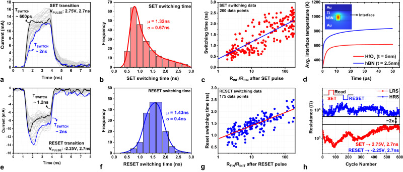
The ability to scale two-dimensional (2D) material thickness down to a single monolayer presents a promising opportunity to realize high-speed energy-efficient memristors. Here, we report an ultra-fast memristor fabricated using atomically thin sheets of 2D hexagonal Boron Nitride, exhibiting the shortest observed switching speed (120 ps) among 2D memristors and low switching energy (2pJ). Furthermore, we study the switching dynamics of these memristors using ultra-short (120ps-3ns) voltage pulses, a frequency range that is highly relevant in the context of modern complementary metal oxide semiconductor (CMOS) circuits. We employ statistical analysis of transient characteristics to gain insights into the memristor switching mechanism. Cycling endurance data confirms the ultra-fast switching capability of these memristors, making them attractive for next generation computing, storage, and Radio-Frequency (RF) circuit applications.


Conflict of interest statement

The authors declare no competing interests.

Figures

Fig. 1
Fig. 1. Device structure of the fabricated 2D hBN memristor.
a Schematic drawing of the memristor device. b Cross-section schematic showing the metal contact used for top (titanium) and bottom electrodes (gold). c SEM image of the device after fabrication (inset) zoomed image where top and bottom electrodes cross. d Phase contrast TEM image of the device cross-section showing 8 layer thick hBN sandwiched between metal electrodes. e Magnified TEM cross-section showing the layered structure of hBN with single-atom defects (arrows) and few atom wide amorphous regions (dashed circles).
Fig. 2
Fig. 2. DC characterization of the 2D hBN memristor.
a DC I–V sweeps of the hBN memristors shown for 20 consecutive cycles (SET curves shown in red traces and RESET curves shown in blue traces). b Cumulative probability distribution of the resistance in HRS and LRS states extracted from DC sweeps at VREAD = 0.1 V collected from 200 I–V traces. c SET/RESET voltage distribution using 100uA compliance current. d SET I–V curve plotted on log-log scale shows regions with varying slope in HRS and linear slope in LRS. e I–V sweep of the device in LRS measured at various operating temperatures (225 K (pink curve), 250 K (black curve), 275 K (blue curve), 300 K (red curve)); (inset) resistance extracted at VREAD = 0.5 V plotted vs. temperature. The memristor in LRS has a positive temperature coefficient of resistance indicating the formation of metallic filaments (f) I–V sweeps of the device in HRS measured at various operating temperatures (225–300 K); (inset) resistance extracted at VREAD = 0.5 V (black curve),0.75 V (blue curve),1 V (red curve) plotted vs. temperature. Reducing resistance with increasing temperature suggests conduction through insulating medium. g TEM cross-section illustrating the locations where electron energy loss spectroscopy (EELS) profile was collected. Points A (red curve), D (black curve) are located inside Au electrode, point B (blue curve) is located inside hBN layer, and point C (green curve) inside Ti electrode.
Fig. 3
Fig. 3. Ultra-fast pulse characterization setup and waveforms.
a Schematic drawing of the high-frequency pulse test setup; (right) zoomed schematic of the probe tips with 50 Ω termination for maximum power transfer .b Applied voltage pulse (black trace) and measured current (red trace) waveform for SET operation. The applied pulse has a pulse-width of 2.7 ns and the device switches in about 700 ps, c I–V plot of the data in (b) shows change in resistance during the applied pulse. d Applied voltage pulse (black trace) and measured current (blue trace) waveform for RESET operation (e) I–V plot of the data in (d) shows change in resistance during the applied pulse.
Fig. 4
Fig. 4. Statistical analysis of transient switching characteristics using ultra-fast pulses.
a Measured current waveforms on 30 different devices under identical applied voltage pulses (VPULSE → 2.75 V, 2.7 ns) during SET operation. b SET switching time distribution created from 200 measurements with a mean value of 1.32 ns. c Correlation between SET switching time and resulting relative change in resistance values. Large resistance change requires a longer switching time. d Transient response of average interface temperature for 2.5 nm thick hBN and 5 nm thick HfOx, obtained through COMSOL simulation (inset) snapshot of temperature heatmap. e Measured current waveforms on 30 devices under identical applied voltage pulses (VPULSE→ −2.25 V, 2.7 ns) during RESET operation. f RESET switching time distribution created from 175 measurements with a mean value of 1.43 ns. g Correlation between RESET switching and resulting relative change in resistance after the RESET pulse. h Switching endurance measurement of single device demonstrates 600 cycles with 2.7 ns pulses (SET data points shown in red and RESET data points shown in blue).
Fig. 5
Fig. 5. Statistical analysis of memristor switching energy.
a Schematic representation of the partition between switching energy and excess energy. b SET switching energy distribution created from 200 measurements with a mean of 25.1 pJ. c Resistance distribution of RINIT (red box plot), RPUL (blue box plot), and RFIN (green boxplot) (inset) waveform illustrating the time instance at which the resistances were measured. The distribution clearly indicates the filament resistance increases after pulse termination. d Relative resistance change after SET pulse variation vs excess energy expended in the device. Since excess energy is proportional to the Joule heating in the device, higher excess energy results in narrowing of the filament. e RESET switching energy distribution created from 175 measurements with a mean of 22.9 pJ. f Relative resistance change after RESET pulse vs switching energy.
Fig. 6
Fig. 6. Demonstration of highest switching speed in 2D memristors.
a Applied SET voltage pulse (gray trace) and measured current (red trace) for thin hBN (3–4 layers) memristor. The pulse-width of the voltage pulse is about 120 ps. b Applied RESET voltage pulse (gray trace) and measured current (blue trace) using 120 ps pulse. c Endurance cycling between LRS and HRS of the memristor with ultra-short pulses. The device shows 100 consecutive cycles of consistent switching, which is the highest ever reported endurance using ultra-short pulses. d Plot benchmarking the performance of the devices presented in this article with other TMO and 2D material memristors.

References

    1. Talib MA, Majzoub S, Nasir Q, Jamal D. A systematic literature review on hardware implementation of artificial intelligence algorithms. J. Supercomput. 2021;77:1897–1938. doi: 10.1007/s11227-020-03325-8. - DOI
    1. Capra M, et al. An updated survey of efficient hardware architectures for accelerating deep convolutional neural networks. Future Internet. 2020;12:113. doi: 10.3390/fi12070113. - DOI
    1. Stoica, I. et al. A Berkeley view of systems challenges for Preprint at https://arxiv.org/abs/1712.05855 (2017).
    1. Pereira F, Correia R, Pinho P, Lopes SI, Carvalho NB. Challenges in resource-constrained IoT devices: energy and communication as critical success factors for future IoT deployment. Sensors. 2020;20:6420. doi: 10.3390/s20226420. - DOI - PMC - PubMed
    1. Fan X, et al. Flexible and wearable power sources for next‐generation wearable electronics. Batteries Supercaps. 2020;3:1262–1274. doi: 10.1002/batt.202000115. - DOI