Review
. 2024 Feb 8;8(3):2300306.
doi: 10.1002/gch2.202300306. eCollection 2024 Mar.

Innovative Strategies for Photons Management on Ultrathin Silicon Solar Cells

Affiliations
Review

Innovative Strategies for Photons Management on Ultrathin Silicon Solar Cells

Ning Li et al. Glob Chall. .

Abstract

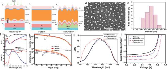
Silicon (Si), the eighth most common element in the known universe by mass and widely applied in the industry of electronics chips and solar cells, rarely emerges as a pure element in the Earth's crust. Optimizing its manufacturing can be crucial in the global challenge of reducing the cost of renewable energy modules and implementing sustainable development goals in the future. In the industry of solar cells, this challenge is stimulating studies of ultrathin Si-based architectures, which are rapidly attracting broad attention. Ultrathin solar cells require up to two orders of magnitude less Si than conventional solar cells, and owning to a flexible nature, they are opening applications in different industries that conventional cells do not yet serve. Despite these attractive factors, a difficulty in ultrathin Si solar cells is overcoming the weak light absorption at near-infrared wavelengths. The primary goal in addressing this problem is scaling up cost-effective and innovative textures for anti-reflection and light-trapping with shallower depth junctions, which can offer similar performances to traditional thick modules. This review provides an overview of this area of research, discussing this field both as science and engineering and highlighting present progress and future outlooks.

Keywords: anti‐reflection; light‐trapping; power conversion efficiency; solar cell; ultrathin silicon.


Conflict of interest statement

The authors declare no conflict of interest.

Figures

Figure 1
Figure 1
Single‐pass absorption of a planal layer of Si with varying thickness of (orange solid line) 10 µm, and (green solid line) 180 µm. We report the solar power density spectrum for reference in the solid blue line.
Figure 2
Figure 2
a) Optical image and schematic of a 10‐µm‐thick crystalline Si photovoltaic cell with an integrated periodic surface light‐trapping structure. b) SEM cross‐section of the complete device. c–e) Experimentally measured (c) absorptance, (d) EQE, and (e) current density–voltage (JV) characteristics of devices A (highest efficiency) and B (highest current) and a planar reference cell. The data plotted in (c) displays total absorption, which includes parasitic absorption in the Al and Si nitride layers; simulated parasitic Al absorption plotted using results from transfer matrix method calculations. Ideal Lambertian absorption plotted for a 10‐µm‐thick Si slab using Si optical indices from ref. [74]. Reproduced with permission.[ 31 ] Copyright 2015, Wiley‐VCH.
Figure 3
Figure 3
a) Complete structure of patterned c‐Si solar cell on glass. b) Colorized SEM image of the cross‐section of the complete stack of a patterned solar cell on glass. From bottom to top: glass substrate, metallic back contact/mirror (purple), ZnO:Al optical spacer (green), n‐type μc‐SiOx:H passivation layer (red), c‐Si epilayer, p‐type a‐Si:H passivation layer (red), ITO (blue), top metallic contact (yellow). c) Current–voltage characteristics of 3 µm thick planar (blue) and patterned (red) c‐Si solar cells on glass under one sun illumination. d) EQE measurements of planar and patterned solar cells, double‐pass absorption calculated for a Si slab of the same thickness d = 3 µm, and specular reflectivity R plotted as (1 – R). e) FDTD calculated absorption in each layer of a patterned solar cell (yellow: Si epilayer, black: Ag mirror, green: ZnO:Al optical spacer, brown: back passivation layer, red: top passivation layer, blue: ITO). The envelope represents the total absorption. f) Schematic of a simplified model for the solar cell. g) Comparison of the EQE of solar cells with nanopyramid arrays with different models: double‐pass absorption with F = 2 (flat cell) and F = 2 × 1.25 (effective thickness induced by diffraction), and propagation model with F = 10. The propagation model is plotted on the whole wavelength range (dotted red curve), with the domain of validity highlighted in solid red. Reproduced with permission.[ 32 ] Copyright 2016, American Chemical Society.
Figure 4
Figure 4
a) Schematic illustration of the solar cell device. b) SEM images of the cross‐sectional view of the nanocones. The thin layer at the top of the nanocones is an 80‐nm‐thick SiO2 layer. Scale bar is 400 nm. c) EQE data of the device and a planar control. d) JV characteristics of the device and a planar control. e) Calculated EQE data of four different 10‐µm‐thick devices with the front–back‐contact and all‐back‐contact designs. f) Light absorption data of three devices. The anti‐reflection layer is Si3N4 with a thickness of 80 nm. Reproduced with permission.[ 5 ]. Copyright 2013, Nature Publishing Group.
Figure 5
Figure 5
a) Schematic structure of a LARC ultrathin solar cell device. b,c) Optical microscopy image (left) and SEM image (right) of the top surface of the solar cells with (b) a single‐nanoblock anti‐reflection coating (ARC) and (c) a double‐nanoblock LARC. d,e) Schematics structure of (d) a single‐nanoblock ARC and (e) a double‐nanoblock LARC. f) JV characteristics of solar cell devices with different photon trapping systems: a double‐nanoblock LARC (red), a single‐nanoblock ARC (blue), a conventional SiNx ARC (green), and planar reference without an ARC (grey). The orange curve shows the highest efficiency cell with a double‐nanoblock LARC on a different wafer. g) Measured reflectance spectra of ultrathin c‐Si solar cells with single (blue) and double (red) nanoblocks‐arrays, SiNx ARC (green), and without ARC (grey). Inset: SEM image of the cross‐section of the single‐nanoblock array with a thermal SiO2 passivation layer (light blue). h) Measured EQE spectra of ultrathin c‐Si solar cells with different light‐trapping textures. i) Measured EQE of the solar cell with the double‐nanoblock array as a function of incident angle and wavelength. Reproduced with permission.[ 24 ] Copyright 2023, Wiley‐VCH.
Figure 6
Figure 6
a) Device structure of thin film c‐Si/PEDOT:PSS hybrid solar cells with surface texturing of reconstructed‐SiNPs combined with highly doped BSF layer (N+‐Si). b) Cross‐sectional SEM images of SiNPs after the first round of the MaCE process and c) after the second round of the MaCE process. The insets in (b,c) show the top view of SiNPs after the first and second rounds of the MaCE process, respectively. d) Reflection spectra of 20 µm thick thin film c‐Si with flat, conventional‐SiNP, and reconstructed‐SiNP surface texturing in the whole wavelength range. e) Averaged reflectance in the full wavelength range of conventional‐SiNPs and reconstructed‐SiNPs at different AOIs. f) Current density–voltage (JV) curves of thin film Si/PEDOT:PSS HHSCs with different surface texturing. g) EQE measurements results of thin film Si/PEDOT:PSS HHSCs with different surface texturing. h) JV curves of the BSF‐combined 20 µm thick c‐Si/PEDOT:PSS HHSCs with and without surface texture. Reproduced with permission.[ 57 ] Copyright 2015, American Chemical Society.
Figure 7
Figure 7
a) SEM images of the NC‐NPs array after the fourth‐round chemical reconstruction. b) The scale bar in (a) is 1 µm, and in (b) is 5 nm. c) Reflection curves of reconstructed NPs arrays with different etching cycles. d) Schematics of hexagonal arrays of Si nanostructures with NC‐NPs configurations and individual hexagonal structures. e,f) Optical photocurrent losses JR_loss variation of NPs and NC‐NPs arrays with different FR and different P in the wavelength range of (e) 300–800 nm and (f) 800–1200 nm. g–i) JR_loss variation of NC‐NPs arrays with different NCs heights in the wavelength range of (g) 300–800 nm and (h) 800–1200 nm. i) Simulated absorption curves of NPs, NCs, and NC‐NPs array with 10 µm‐thick c‐Si substrate and a Lambertian limit of Si film with equal thickness. j) NP, NC, and NC‐NP structure absorption profiles at the wavelength of 400 nm. k) Current–voltage JV curves and l) EQE characteristics of the three types of solar cells. Reproduced with permission.[ 20 ] Copyright 2016, Wiley‐VCH.
Figure 8
Figure 8
a–c) Schematic device structures of the n‐i‐p a‐Si:H solar cells deposited on the (a) plasmonic, (b) flat, and (c) textured BRs. SEM image (d) and size distribution (e) of Ag NPs. f) Total reflectance R and haze in reflection of flat, plasmonic, and textured BRs. g) Angular intensity distribution of light scattered by plasmonic and textured BRs at the wavelength of 600, 700, and 800 nm. h) EQE curves of plasmonic and textured n‐i‐p a‐Si: solar cells and textured p‐i‐n a‐Si:H solar cell fabricated on the Asahi VU‐type glass. i) JV curves of flat, plasmonic, and textured n‐i‐p a‐Si:H solar cells, and textured p‐i‐n a‐Si:H solar cells. Reproduced with permission.[ 60 ] Copyright 2012, American Chemical Society.

References

    1. N. RILEY , The cost of solar panels: Is it worth it?, 2022, https://www.investopedia.com/articles/mortgages-real-estate/10/solar-pow....
    1. Taylor M., Al‐Zoghoul S., Ralon P., Sorokina O., IRENA , Renewable power generation costs in 2022, International Renewable Energy Agency, Abu Dhabi, 2023.
    1. Butler D., Nature 2008, 454, 558. - PubMed
    1. Goodrich A., Hacke P., Wang Q., Sopori B., Margolis R., James T. L., Woodhouse M., Sol. Energy Mater. Sol. Cells 2013, 114, 110.
    1. Jeong S., McGehee M. D., Cui Y., Nat. Commun. 2013, 4, 2950. - PubMed

LinkOut - more resources