. 2024 Mar 16;15(1):2386.
doi: 10.1038/s41467-024-46615-y.

Three-dimensional ultrafast charge-density-wave dynamics in CuTe

Affiliations

Three-dimensional ultrafast charge-density-wave dynamics in CuTe

Nguyen Nhat Quyen et al. Nat Commun. .

Abstract

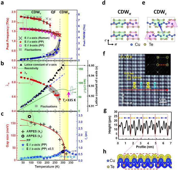
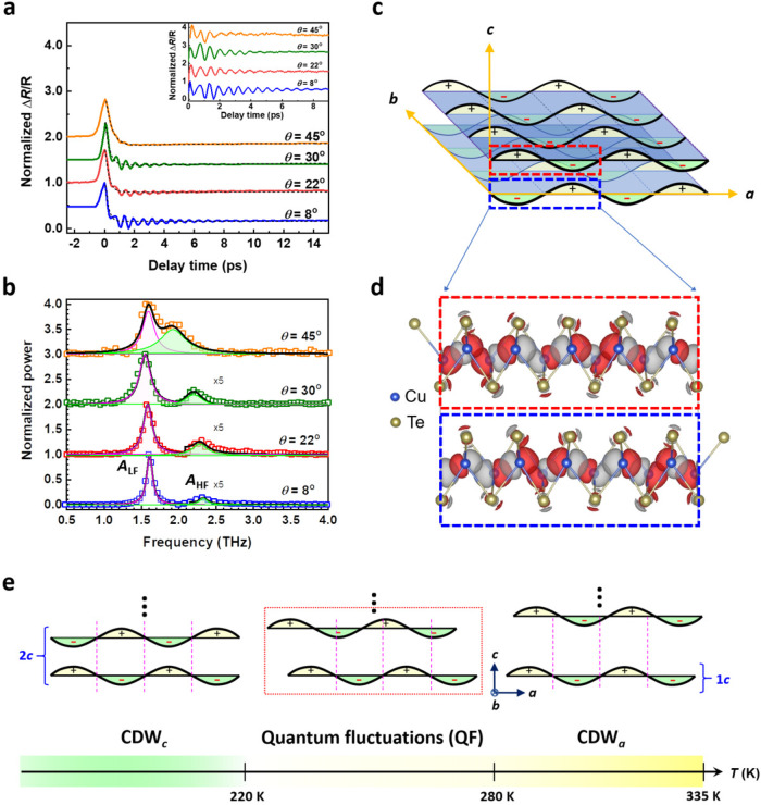
Charge density waves (CDWs) involved with electronic and phononic subsystems simultaneously are a common quantum state in solid-state physics, especially in low-dimensional materials. However, CDW phase dynamics in various dimensions are yet to be studied, and their phase transition mechanism is currently moot. Here we show that using the distinct temperature evolution of orientation-dependent ultrafast electron and phonon dynamics, different dimensional CDW phases are verified in CuTe. When the temperature decreases, the shrinking of c-axis length accompanied with the appearance of interchain and interlayer interactions causes the quantum fluctuations (QF) of the CDW phase until 220 K. At T < 220 K, the CDWs on the different ab-planes are finally locked with each other in anti-phase to form a CDW phase along the c-axis. This study shows the dimension evolution of CDW phases in one CDW system and their stabilized mechanisms in different temperature regimes.


Conflict of interest statement

The authors declare no competing interests.

Figures

Fig. 1
Fig. 1. Experimental scheme and orientation-resolved ultrafast spectra for CuTe.
Left: Orientation-dependent transient reflectivity change (ΔR/R) spectra on the ab-plane of a CuTe single crystal from ϕ1 (ϕ2) = 0° (a-axis) to 90° (b-axis) at 37 K. Right: Crystal structure of CuTe and schematics of the orientation-/time-resolved ultrafast spectroscopy. a: a-axis. b: b-axis. c: c-axis. t is the delay time between the pump and probe pulses. θ is the angle between the c-axis of a (001) CuTe single crystal and the incident direction of the probe beam. ϕ1 and ϕ2 are the angles between the a-axis of a (001) CuTe single crystal and the respective polarization of the pump and probe pulses.
Fig. 2
Fig. 2. Ultrafast dynamics at various temperatures.
a ΔR/R along a-axis (θ = 8°, ϕ1 and ϕ2 = 0°) of a CuTe single crystal at various temperatures. Inset: a typical oscillation component of ΔR/R spectra at 37 K after subtracting the decay background (dashed line fitted by Eq. (1)). b Spectrogram of the oscillation components at 37 K and 280 K in (a) after short-time Fourier transformation. c, d Simulated the oscillation components of ΔR/R spectra (black and solid circles are experimental data in (a)) at low (e.g., TeL = 37 K) and high (e.g., TeH = 280 K) temperatures in (a) using the TDGL equation, Supplementary Eq. (1). V(Te, t): the ground-state double-well potential as a function of electron temperature Te and delay time t. V(TeL0(eH0), t0): the high-symmetry state at zero delay time t0 for lower (higher) electron temperature TeL0 (TeH0) after pumping. V(TeL1(eH1), t1): the double-well potential at delay time t1 for lower (higher) electron temperature TeL1 (TeH1) after relaxation.
Fig. 3
Fig. 3. Temperature evolution and spatial modulation for CDW orders.
a Frequency/full width at half maximum (FWHM of 1.64-THz peak at 37 K) for peaks in the Fourier transform spectra in Fig. 2a (for E//b-axis from Supplementary Fig. 3) and Raman modes (obtained from Supplementary Fig. 4) as a function of temperature. Solid lines show the fitting results using the TDGL equation, Supplementary Eq. (2). QF: quantum fluctuations. PP: pump-probe spectra. The shaded area marks the fluctuations in the data. The error bars are obtained from the standard deviation of the least square fitting. b Electron-phonon coupling constant λa (solid squares) as a function of temperature, which is derived by fitting the data in (a) with Supplementary Eq. (2). The solid line represents the resistivity of CuTe as a function of temperature. Solid triangles show the temperature-dependent lattice constant for the c-axis of CuTe. Dashed lines are guides for the eyes. The shaded area marks the fluctuations in data. c Relaxation time τe for photoexcited electrons as a function of temperature and obtained by fitting the ΔR/R spectra in Fig. 2a (Supplementary Fig 3a for b-axis) with Eq. (1). CDW gap size as a function of temperature. PP: obtained by fitting the τe data with the mean-field-like model (a gray-thick line). ARPES (kx): obtained from the ARPES images in Supplementary Fig. 5. ARPES (kz): obtained from the ARPES images in Supplementary Fig. 6. d, e Modulated structure and eigenvectors in the CDW along the a-axis (CDWa) and CDW along the c-axis (CDWc) that is proposed by first-principles simulations. f High-resolution STM image of as-cleaved CuTe surface (Vs = 300 mV, It = 6.79 nA) in real space. The yellow rectangle indicates a unit cell of CuTe. Inset: 2D fast Fourier transform image of the STM image in (f). Yellow circles mark the points of a 1 × 1 unit cell, and the red circles represent the 5 × 1 CDW modulated superstructure. g The line profile along the red-dashed arrow in (f). h Charge density isosurface (with a value of 0.032 e/bohr3) of a CuTe layer building block, which is obtained using first-principles calculations.
Fig. 4
Fig. 4. Ultrafast dynamics along the c-axis of CuTe and schematics of a CDW in various dimensions.
a Normalized ΔR/R spectra of a CuTe single crystal at different incident angles, θ (ϕ1 and ϕ2 = 0°) at T = 100 K. Inset: the oscillation components of normalized ΔR/R spectra in (a) after subtracting the decay background (dashed line fitted using Eq. (1)). b Fourier transform spectra of the oscillation components in the inset of (a). c Schematics of a CDW in various dimensions for which two layers along the c-axis are anti-phase. d Modulated structure of the CDW in (c) with charge density difference between CDWc and non-CDW (normal) states obtained by first-principles calculations. An absolute isosurface value of 0.007 e/bohr3 is adopted, whereas the positive and negative charge differences are, respectively, denoted as red and gray clouds (for details, see Supplementary Note 6). e The dimension evolution of CDW phases from high to low temperatures in CuTe.

References

    1. Liu G, et al. A charge-density-wave oscillator based on an integrated tantalum disulfide-boron nitride-graphene device operating at room temperature. Nat. Nanotechnol. 2016;11:845–850. doi: 10.1038/nnano.2016.108. - DOI - PubMed
    1. Vaskivskyi I, et al. Fast electronic resistance switching involving hidden charge density wave states. Nat. Commun. 2016;7:11442. doi: 10.1038/ncomms11442. - DOI - PMC - PubMed
    1. Travaglini G, Wachter P. Charge-density-wave-phase-mode evidence in one-dimensional K0.3MoO3. Phys. Rev. B. 1984;30:1971–1978. doi: 10.1103/PhysRevB.30.1971. - DOI
    1. Vescoli V, Degiorgi L, Berger H, Forró L. Dynamics of correlated two-dimensional materials: the 2H-TaSe2 case. Phys. Rev. Lett. 1998;81:453. doi: 10.1103/PhysRevLett.81.453. - DOI
    1. Yoshikawa N, et al. Ultrafast switching to an insulating-like metastable state by amplitudon excitation of a charge density wave. Nat. Phys. 2021;17:909–914. doi: 10.1038/s41567-021-01267-3. - DOI