. 2024 Mar 25:10:44.
doi: 10.1038/s41378-024-00674-9. eCollection 2024.

Nanofabricated high turn-density spiral coils for on-chip electromagneto-optical conversion

Affiliations

Nanofabricated high turn-density spiral coils for on-chip electromagneto-optical conversion

Ilhan Bok et al. Microsyst Nanoeng. .

Abstract

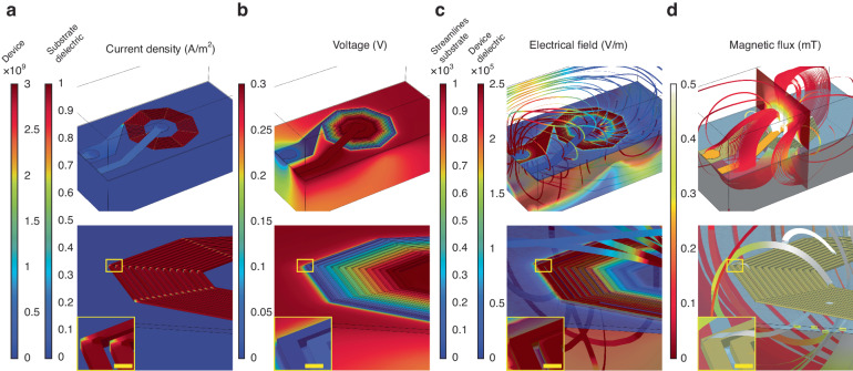
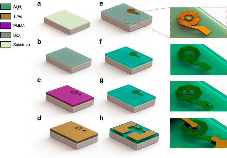
Circuit-integrated electromagnets are fundamental building blocks for on-chip signal transduction, modulation, and tunability, with specific applications in environmental and biomedical micromagnetometry. A primary challenge for improving performance is pushing quality limitations while minimizing size and fabrication complexity and retaining spatial capabilities. Recent efforts have exploited highly involved three-dimensional synthesis, advanced insulation, and exotic material compositions. Here, we present a rapid nanofabrication process that employs electron beam dose control for high-turn-density diamond-embedded flat spiral coils; these coils achieve efficient on-chip electromagnetic-to-optical signal conversion. Our fabrication process relies on fast 12.3 s direct writing on standard poly(methyl methacrylate) as a basis for the metal lift-off process. Prototypes with 70 micrometer overall diameters and 49-470 nm interturn spacings with corresponding inductances of 12.3-12.8 nH are developed. We utilize optical micromagnetometry to demonstrate that magnetic field generation at the center of the structure effectively correlates with finite element modeling predictions. Further designs based on our process can be integrated with photolithography to broadly enable optical magnetic sensing and spin-based computation.

Keywords: Nanoscale devices; Sensors.


Conflict of interest statement

Conflict of interestThe authors declare no competing interests.

Figures

Fig. 1
Fig. 1. Modeled electromagnetic behavior of the device.
Nanofabricated spiral coil design and predicted performance on high resistivity substrate are evaluated via finite element analysis in response to the input current injected through the dielectric and the coil center. a Stimulation-driven current density (A/m2) in the device is predictably greater than that in the surrounding substrate and dielectric material. Bottom and inset, enlarged regions demonstrating the details of individual coil turns. b Corresponding voltage (V) reaches 0.3 V in response to the current density shown in (a). c Resulting electrical field (V/m) in the substrate and device dielectric. d Magnetic flux (mT) is determined when the current injection reaches > 0.5 mT in the coil center. Streamlines are tangent to the vector field representing the electrical field within the model space. Shown are cross-sections of the model space and streamlines around the device. Scale bars are 1 µm for all insets in (a)-(d). Interturn spacings (s) ranging between 49 and 470 nm are demonstrated in the remainder of this study
Fig. 2
Fig. 2. Fabrication process overview.
a The device is fabricated on resistive glass or diamond substrates. b A 100 nm thick SiO2 barrier layer is deposited on the surface. c A 400 nm PMMA layer is spin coated and patterned via EBL to define the nanocoil features. d A Ti/Au (6/60 nm) bilayer is deposited via e-beam evaporation and subsequently lifted off to create a coil structure (e). f An additional insulating SiO2 layer is deposited to prepare for PL micropatterning via electrode routing. g Via holes are defined via PL and etched with a fluorine-based plasma recipe. h Finally, patterns for electrode traces are fabricated, and gold electrodes are laid via evaporation and lift-off. The samples are further packaged and routed onto glass printed circuit boards for magnetometry
Fig. 3
Fig. 3. Dose-dependent feature analysis of nanofabricated spiral coils.
a A complete view of the end device. The dotted red region is a scanning electron microscopy (SEM) image of the EBL step in the left inset, showing distinct uniformity of turns for a dose of 1120 µC/cm2 (scale bar = 5 µm). Different doses with the closest corresponding AFM traces are shown in (b): 960 µC/cm2 (left), 1280 µC/cm2 (center), and 1600 µC/cm2 (right; scale bar = 5 µm), with corresponding 3-dimensional AFM traces color-coded by height (insets). c Single-pixel Monte Carlo simulation of PMMA exposure where 1 Gy ≡ 7.366 eV/cm3 and d corresponding triple-turn simulation color-coded by particle trajectory height. The gold, magenta, and cream-colored layers correspond to gold, PMMA, and quartz, respectively. e Average turn widths and gap widths versus dose, determined using atomic force microscopy, showing a linear relationship between dose and feature size. Shown on the right is a matrix comparing (f) single-pixel Monte Carlos, g multiturn Monte Carlos, h (with zoomed regions of interest), i PMMA pre-liftoff, j (with close-up ROIs), and k Ti/Au post-liftoff, l (with close-up ROIs). The columns from left to right correspond to doses of 320, 480, 640, 800, 960, 1120, 1280, 1440, and 1600 µC/cm2 (scale bar = 500 nm (overview panels) or 100 nm (zoomed ROIs))
Fig. 4
Fig. 4. Nanocoil feature measurements and fitness calculations.
a Finite element analysis (cyan) reveals slope trends in agreement with the AFM (pink) and SEM (red) measurements. The inset shows an example of support vector machine (SVM) regression of a PMMA slope. Blue and orange dots represent mesh points with subthreshold and suprathreshold exposure, respectively. The solid line and dashed lines represent the optimal hyperplane and margin, respectively. b Whole-coil resistance and c parasitic interturn capacitance. Wheeler method and sheet spiral inductance calculations are shown in (d), with the corresponding self-resonance (e) and Q factor (f). All quantities are plotted versus the electron beam dose ranging from 640 to 1440 µC/cm2 except for the SEM data, which extend to 1600 µC/cm2. Comparing the impedance in decibel ohms to the linear frequency reveals a dose-dependent tuning curve (g) with varying resonant frequency and Q factor (inset)
Fig. 5
Fig. 5. Dose-dependent power dissipation quantification and analysis.
a Full view of the nanocoil (dose: 640 µC/cm2) with the coil surface color coded by the x-component of the Poynting vector (Pox) and the plane of the coil color coded by the magnetic energy density (J/m3). The red dashed box shows the regions expanded in (g) and (h). Inset: Subtraction histogram between high-dose (1440 µC/cm2) and low-dose (640 µC/cm2) vector counts versus angle color-coded by magnitude. b Vector magnitude for the integral of the X, Y, and Z components ∮∮coilPoxx^+∮∮coilPoyy^+∮∮coilPozz^ over the entire coil surface of dissipated power versus dose examined with lines of best fit affirming a linear trend between the electron beam dose-dependent turn width and dissipated power. ch Two-dimensional (2D) Poynting vector x (Pox), y (Poy) and z (Poz) plots for 640 µC/cm2 (c, e) and 1440 µC/cm2 (d, f) for the dashed boxes in (a) (c, d scale bar = 10 µm) and zoomed inset (red dashed boxes, e, f, scale bar = 1 µm). Three-dimensional (3D) plots of corresponding regions for 640 µC/cm2 (g scale bar = 1 µm) and 1440 µC/cm2 (h scale bar = 1 µm). i Separate surface integrals of the X, Y, and Z components of the Poynting vector demonstrating linear relationships between the electron beam dose-dependent turn width and dissipated power
Fig. 6
Fig. 6. Optical magnetometry measurements of the nanocoil B-field strength during current injection.
a Experimental setup. b, c B-field maps of two different device routing configurations. Top left: reference image with delineated line scans; bottom left: B-field amplitude (0 mA DC); bottom right: B-field amplitude (3 mA DC); top right: current OFF minus current ON subtraction; B-field z component. dg Vector field lines of the B-field gradient overlaid on B-field maps. e and g orrespond to dashed boxes in (d) and (f), respectively. h, i Uniformity maps comprising vector field lines of B-field gradient overlaid on corresponding B-field gradient maps. j Simulation of uniformity map for comparison. k, l 100 µm line scans of the B-field z component for (b) and (c), respectively, taken at y = +25, 0, −25 µm from the device center. Scale bars = 20 µm

References

    1. Burghartz JN, Rejaei B. On the design of RF spiral inductors on silicon. IEEE Trans. Electron Devices. 2003;50:718–729. doi: 10.1109/TED.2003.810474. - DOI
    1. Le HT, et al. MEMS inductor fabrication and emerging applications in power electronics and neurotechnologies. Microsyst. Nanoeng. 2021;7:1–22. doi: 10.1038/s41378-021-00275-w. - DOI - PMC - PubMed
    1. Alibakhshikenari M, et al. A comprehensive survey on antennas on-chip based on metamaterial, metasurface, and substrate integrated waveguide principles for millimeter-waves and terahertz integrated circuits and systems. IEEE Access. 2022;10:3668–3692. doi: 10.1109/ACCESS.2021.3140156. - DOI
    1. Nguyen, C. T.-C. Microelectromechanical devices for wireless communications. in Proceedings MEMS 98. IEEE. Eleventh Annual International Workshop on Micro Electro Mechanical Systems. An Investigation of Micro Structures, Sensors, Actuators, Machines and Systems (Cat. No. 98CH36176) 1–7. 10.1109/MEMSYS.1998.659719 (1998).
    1. O KK, et al. On-chip antennas in silicon ICs and their application. IEEE Trans. Electron Devices. 2005;52:1312–1323. doi: 10.1109/TED.2005.850668. - DOI