Effect of Deposition Working Power on Physical Properties of RF-Sputtered CdTe Thin Films for Photovoltaic Applications
- PMID: 38535683
- PMCID: PMC10975583
- DOI: 10.3390/nano14060535
Effect of Deposition Working Power on Physical Properties of RF-Sputtered CdTe Thin Films for Photovoltaic Applications
Abstract
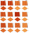
The main objective of this study was to determine the variation in the properties of cadmium telluride (CdTe) thin films deposited on a p-type Si substrate by the radio frequency magnetron sputtering technique at four different working powers (70 W, 80 W, 90 W, and 100 W). The substrate temperature, working pressure, and deposition time during the deposition process were kept constant at 220 °C, 0.46 Pa, and 30 min, respectively. To study the structural, morphological, and optical properties of the CdTe films grown under the mentioned experimental conditions, X-ray diffraction (XRD), scanning electron microscopy (SEM), atomic force microscopy (AFM), and optical spectroscopy were used. For a better analysis of the films' structural and optical properties, a group of films were deposited onto optical glass substrates under similar deposition conditions. The electrical characterisation of Ag/CdTe/Al "sandwich" structures was also performed using current-voltage characteristics in the dark at different temperatures. The electrical measurements allowed the identification of charge transport mechanisms through the structure. New relevant information released by the present study points towards 90 W RF power as the optimum for obtaining a high crystallinity of ~1 μm nanostructured thin films deposited onto p-Si and optical glass substrates with optical and electrical properties that are suitable for use as absorber layers. The obtained high-quality CdTe nanostructured thin films are perfectly suitable for use as absorbers in CdTe thin-film photovoltaic cells.
Keywords: RF–magnetron sputtering (RF–MS); cadmium telluride (CdTe) thin films; current–voltage measurements; physical properties.
Conflict of interest statement
The authors declare no conflict of interest.
Figures


References
-
- National Renewable Energy Laboratory (NREL, USA) Best Research-Cell Efficiency Chart. [(accessed on 24 January 2024)]; Available online: https://www.nrel.gov/pv/cell-efficiency.html.
-
- Sinha T., Lilhare D., Khare A. A review on the improvement in performance of CdTe/CdS thin-film solar cells through optimization of structural parameters. J. Mater. Sci. 2019;54:12189–12205. doi: 10.1007/s10853-019-03651-0. - DOI
-
- Clover I. First Solar Raises Bar for CdTe with 21.5% Efficiency Record. 2015. [(accessed on 24 January 2024)]. Available online: https://www.pv-magazine.com/2015/02/06/first-solar-raises-bar-for-cdte-w...
-
- Duenow J.N., Metzger W.K. Back-surface recombination, electron reflectors and paths to 28% efficiency for thin-film photovoltaics: A CdTe case study. J. Appl. Phys. 2019;125:053101. doi: 10.1063/1.5063799. - DOI
-
- Metzger W.K., Grover S., Lu D., Colegrove E., Moseley J., Perkins C.L., Li X., Mallick R., Zhang W., Malik R., et al. Exceeding 20% efficiency with in situ group V doping in polycrystalline CdTe solar cells. Nat. Energy. 2019;4:837–845. doi: 10.1038/s41560-019-0446-7. - DOI
LinkOut - more resources
Full Text Sources
Miscellaneous

